Chip-scale package

a chip-scale, package technology, applied in the direction of semiconductor devices, semiconductor/solid-state device details, electrical equipment, etc., can solve the problem of adverse effects on the quality of the final produ

Inactive Publication Date: 2009-04-28
INFINEON TECH AMERICAS CORP
View PDF59 Cites 2 Cited by
  • Summary
  • Abstract
  • Description
  • Claims
  • Application Information

AI Technical Summary

Benefits of technology

[0007]In a process according to the present invention, a frame is formed inside a conductive can which is not capable of being wet by solder in liquid phase. The frame so formed defines a die receiving area. A solder paste mass is interposed between the die receiving area and the electrode of a die and reflown. That is, the solder paste may be deposited inside the can and the die placed thereon, or the die may have the solder paste deposited thereon and placed inside the can. Because the frame cannot be wet by the reflown solder (which is in liquid phase), it is contained within the boundary of the frame. As a result, the die is prevented from moving inside the can during the reflow process.
[0010]It has been observed that a frame formed according to the present invention improves the placement accuracy of the die in a can. Furthermore, it has been observed that the die can be effectively centered within the can and aligned with the sidewalls of the can.
[0011]In another embodiment, a dielectric material with high thermal absorption characteristics is deposited on the exterior surface of the can. The dielectric material may be a polymer which can be drop-on-demand deposited onto the exterior surface of the can. To enhance the absorption capability of the dielectric, it may be pigmented with dark or black pigments.

Problems solved by technology

As a result, the quality of the final product may be adversely affected.

Method used


Image

  • Chip-scale package
  • Chip-scale package
  • Chip-scale package

Examples


Embodiment Construction

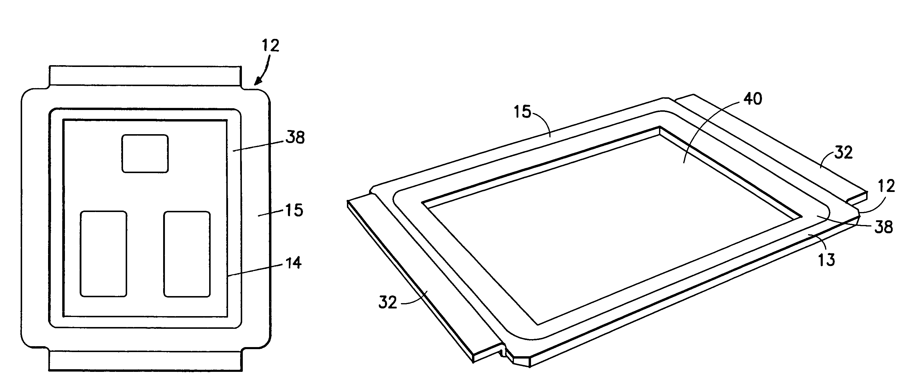
[0023]Referring next to FIGS. 5-8, in a method according to the present invention at least interior surface of web portion 13 of can 12 receives a frame 38 (see FIG. 6). Frame 38 defines a die receiving area 40 inside can 12 on web portion 13 for receiving a semiconductor die, for example, semiconductor die 14 according to the prior art. Next, according to a preferred embodiment, a solder paste mass 42 is deposited on receiving area 40 as illustrated by FIG. 7. Thereafter, a semiconductor die is disposed on solder paste mass 42, and the solder is reflown by heating the arrangement to at least the reflow temperature of solder paste mass 42. Next, the arrangement is cooled whereby the reflown solder paste is hardened to form a conductive adhesive body 18.

[0024]In a process according to an alternative embodiment, solder paste is deposited on an electrode of a semiconductor die, and the die is placed on receiving area 40 with the solder paste disposed between the electrode of the die an...


PUM


Abstract

A method for manufacturing a semiconductor package that includes forming a frame inside a conductive can, the frame being unwettable by liquid solder.

Description

RELATED APPLICATION[0001]This application is based on and claims the benefit of U.S. Provisional Application Ser. No. 60 / 673,160, filed on Apr. 20, 2005, entitled SOLDER MASK INSIDE DIRECT FET CAN, to which a claim of priority is hereby made and the disclosure of which is incorporated by reference.BACKGROUND OF THE INVENTION[0002]The present invention relates to power semiconductor packages and methods of manufacturing power semiconductor packages.[0003]Referring to FIGS. 1-4, a package 10 according to the prior art includes a conductive can 12, and a power semiconductor die 14. Can 12 is typically formed with an electrically conductive material such as copper or a copper-based alloy, and may be coated with silver, gold or the like. Die 14 may be a vertical conduction type power semiconductor MOSFET having its drain electrode 16 electrically and mechanically attached to an interior surface of can 12 by a conductive adhesive 18 such as solder or a conductive epoxy (e.g. silver epoxy)...

Claims


Application Information

Patent Timeline
Patent Type & Authority Patents(United States)
IPC IPC(8): H01L21/00
CPCH01L21/50H01L23/10H01L23/492H01L24/33H01L24/83H01L2224/73153H01L2224/73253H01L2224/83191H01L2224/83192H01L2224/83194H01L2224/83801H01L2224/83851H01L2924/01005H01L2924/01029H01L2924/01033H01L2924/01047H01L2924/0105H01L2924/01079H01L2924/13055H01L2924/13091H01L2924/16152H01L2224/2919H01L2924/01068H01L2924/014H01L2924/0665H01L2924/00H01L2224/291H01L2224/32245H01L2224/26175H01L2224/0603H01L2224/06181
Inventor STANDING, MARTINCLARKE, ROBERT J
Owner INFINEON TECH AMERICAS CORP
Why Eureka
Try Eureka