Thin film magnetic head and method of manufacturing same

a thin film, magnetic head technology, applied in the field of thin film magnetic head, can solve the problems of shortening the manufacturing time and difficult to extremely micrify the pole width with high precision, and achieve the effect of shortening the manufacturing time and a manufacturing method

Inactive Publication Date: 2009-04-28
SAE MAGNETICS (HK) LTD
View PDF7 Cites 3 Cited by
  • Summary
  • Abstract
  • Description
  • Claims
  • Application Information

AI Technical Summary

Benefits of technology

[0008]The invention has been achieved in consideration of the problems. It is a first object of the invention to provide a thin film magnetic head capable of shortening the manufacturing time and a method of manufacturing the same.
[0009]Furthermore, it is a second object of the invention to provide a thin film magnetic head capable of extremely micrifying the pole width with high precision and a method of manufacturing the same.
[0012]In the thin film magnetic head of the invention or the method of manufacturing the same, after the gap layer is formed with the non-magnetic conductive material, at least the first pole tip portion is selectively formed on the gap layer by growing the plating film with the gap layer used as an electrode. Unlike the case where the gap layer is formed with a non-magnetic insulating material, a step of separately forming an electrode layer necessary for growing the plating film aside from the gap layer becomes unnecessary. Therefore, the number of the manufacturing processes is reduced.

Problems solved by technology

However, conventionally, there are problems that it is difficult to shorten the manufacturing time because a lot of manufacturing processes are necessary for manufacturing the thin film magnetic head, and that it is difficult to extremely micrify the pole width with high precision because processing accuracy is not sufficient at the time of etching the write gap layer and the bottom pole in a self-aligned manner.

Method used


Image

  • Thin film magnetic head and method of manufacturing same
  • Thin film magnetic head and method of manufacturing same
  • Thin film magnetic head and method of manufacturing same

Examples


Embodiment Construction

[0032]Hereinbelow, an embodiment of the invention will be described in detail by referring to the drawings.

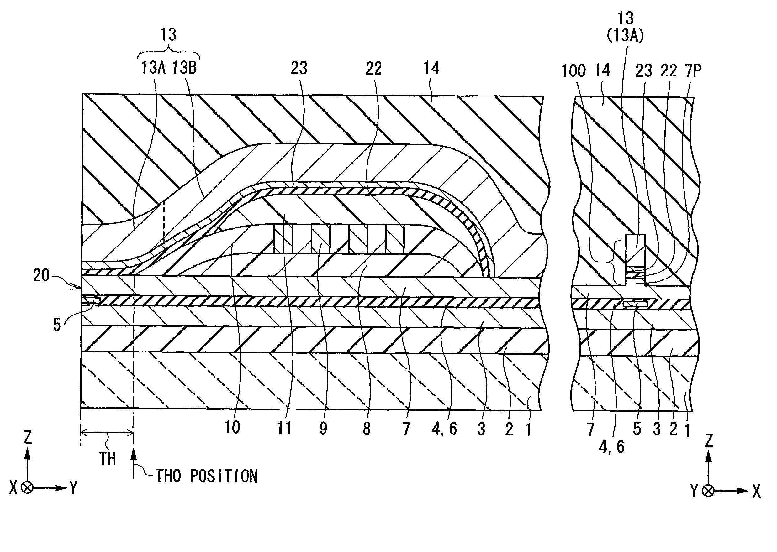
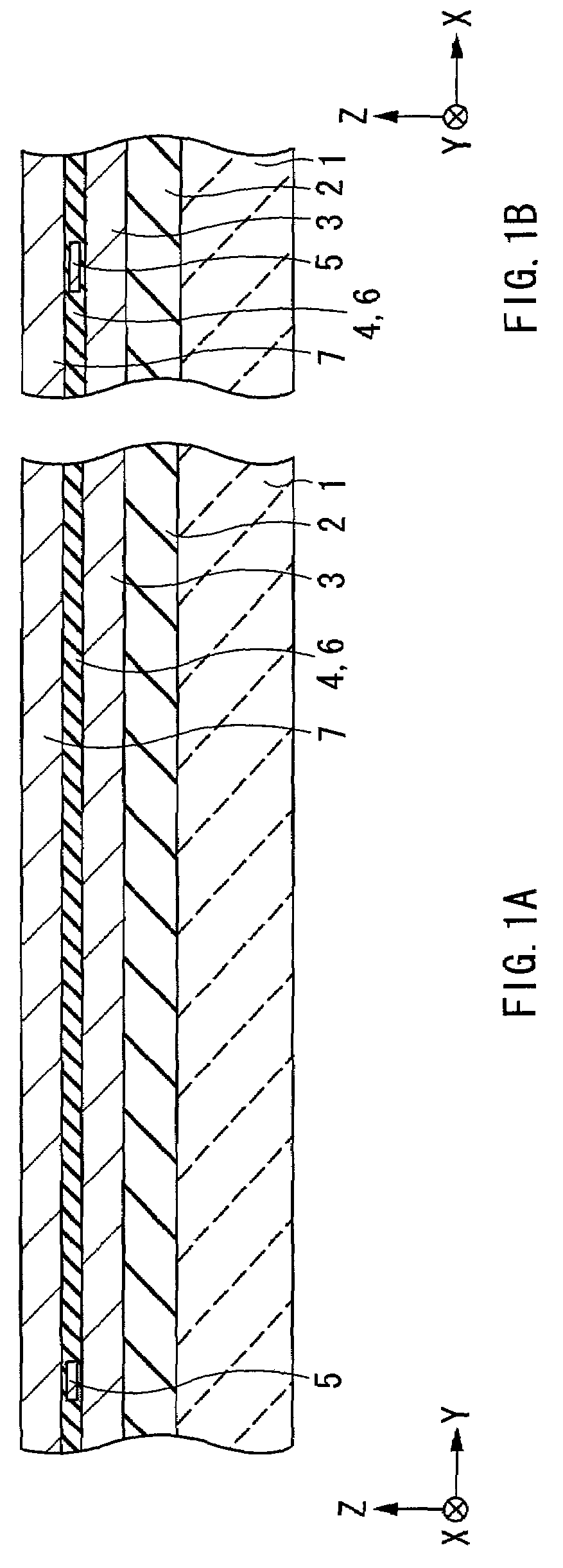
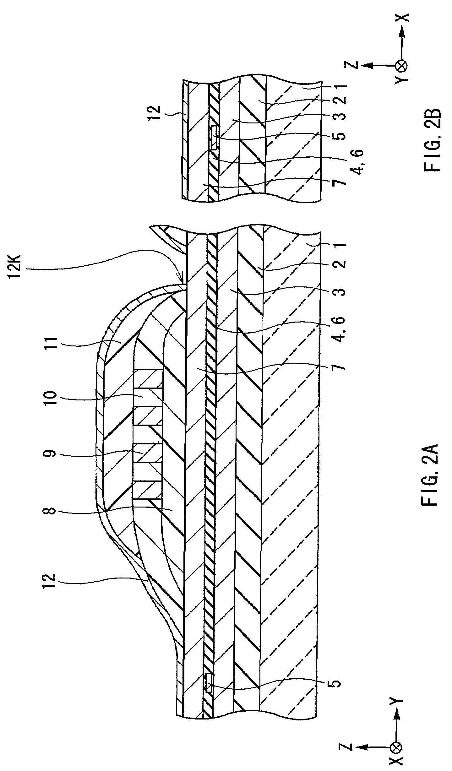
[0033]First, referring to FIGS. 1A and 1B to FIGS. 6A and 6B, and FIGS. 7 to 9, a method of manufacturing a composite thin film magnetic head as “a method of manufacturing a thin film magnetic head” according to an embodiment of the invention will be described. Incidentally, since “a thin film magnetic head” of the invention is embodied by the method of manufacturing the thin film magnetic head according to the embodiment, the head will be also described hereinbelow. FIGS. 1A and 1B to FIGS. 6A and 6B show the method of manufacturing the thin film magnetic head. In each pair of drawings, FIGS. 1A to 6A are cross sections each of which is perpendicular to the air bearing surface, and FIGS. 1B to 6B are cross sections each of which is parallel to the air bearing surface, respectively. FIGS. 7 to 9 show the plane structures corresponding to the cross-sectional structures shown in ...


PUM

PropertyMeasurementUnit
thicknessaaaaaaaaaa
thicknessaaaaaaaaaa
thicknessaaaaaaaaaa

Abstract

A thin film magnetic head capable of shortening a manufacturing time and a method of manufacturing the same are provided. After forming a write gap layer by using a non-magnetic conductive material such as copper, a top pole is formed on the write gap layer by growing a plating film with the write gap layer used as a seed layer. Unlike the case where the write gap layer is formed by using a non-magnetic insulating material such as alumina, a step of newly forming a seed layer aside from the write gap layer and a step of selectively removing the newly formed seed layer become unnecessary. Therefore, the number of manufacturing processes is reduced, and the manufacturing time of the thin film magnetic head is shortened.

Description

BACKGROUND OF THE INVENTION[0001]1. Field of the Invention[0002]The present invention relates to a thin film magnetic head having an inductive magnetic transducer for writing and a method of manufacturing the same.[0003]2. Description of the Related Art[0004]In recent years, an improvement in performance of a thin film magnetic head is demanded in accordance with an increase in areal density of a hard disk drive. As a thin film magnetic head, for example, a composite thin film magnetic head in which a recording head having an inductive magnetic transducer for writing and a reproducing head having a magnetoresistive (hereinbelow, referred to as MR) element for reading are laminated is widely used.[0005]The recording head, for example, comprises: a top pole and a bottom pole which are disposed on the top of, and on the bottom of a write gap, respectively, while sandwiching the write gap made of a non-magnetic insulating material such as aluminum oxide (Al2O3; hereinbelow, simply calle...

Claims


Application Information

Patent Timeline
Patent Type & Authority Patents(United States)
IPC IPC(8): G11B5/127G11B5/23G11B5/235G11B5/31
CPCG11B5/3133G11B5/3163G11B5/232G11B5/235Y10T29/49052Y10T29/49041Y10T29/49048
Inventor MATONO, NAOTO
Owner SAE MAGNETICS (HK) LTD
Why Eureka
Try Eureka