
Semiconductor device and method of manufacturing the same

a technology of semiconductor devices and semiconductors, applied in semiconductor devices, semiconductor/solid-state device details, electrical devices, etc., can solve the problems of poor manufacturing yield and difficulty in shortening manufacturing processes, and achieve the effect of shortening manufacturing processes and

Inactive Publication Date: 2005-07-07
ROHM CO LTD
View PDF10 Cites 11 Cited by
  • Summary
  • Abstract
  • Description
  • Claims
  • Application Information

AI Technical Summary

Benefits of technology

[0012] An object of the present invention is to provide a semiconductor device capable of shortening manufacturing processes and a method of manufacturing the same.
[0013] Another object of the present invention is to provide a semiconductor device whose operating characteristics may not be adversely affected by a heat treatment during manufacturing processes and a method of manufacturing the same.

Problems solved by technology

Therefore, the heat treatment must be carried out at least twice, thereby making it difficult to shorten the manufacturing processes.
Therefore, the operating characteristics of the Schottky barrier diode may be adversely affected by the heat treatment during the manufacturing processes, resulting in poor manufacturing yields.

Method used

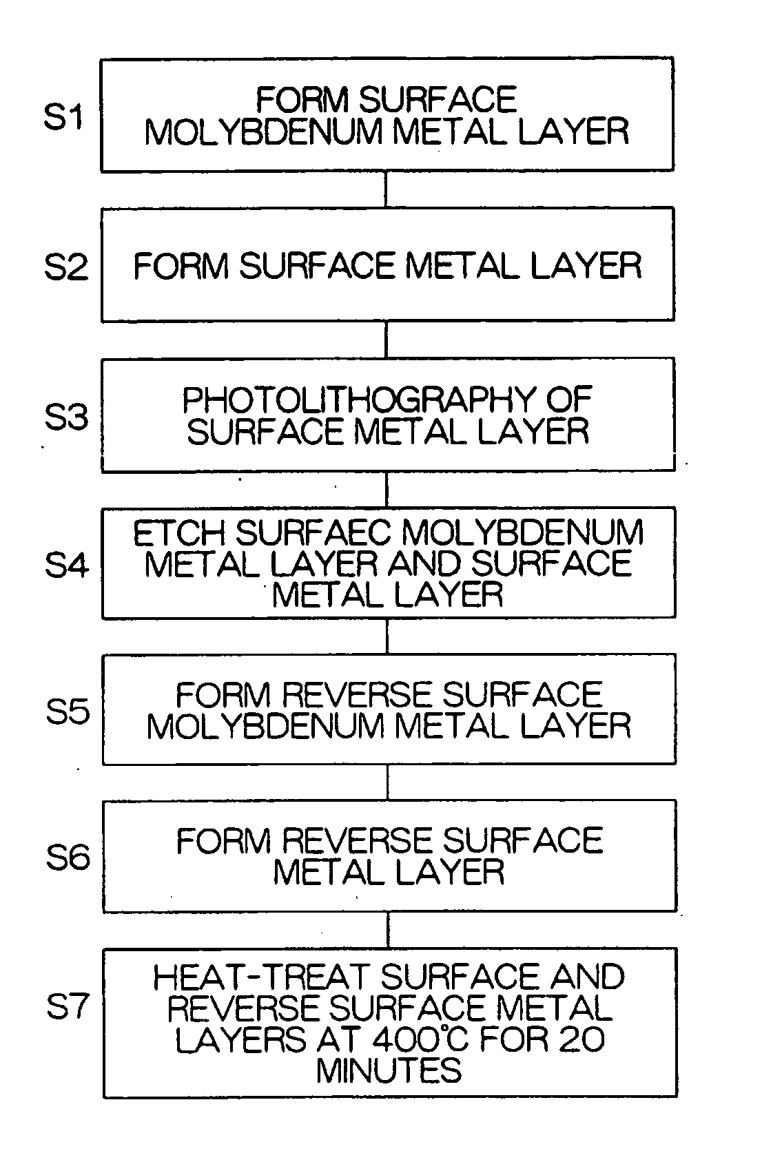
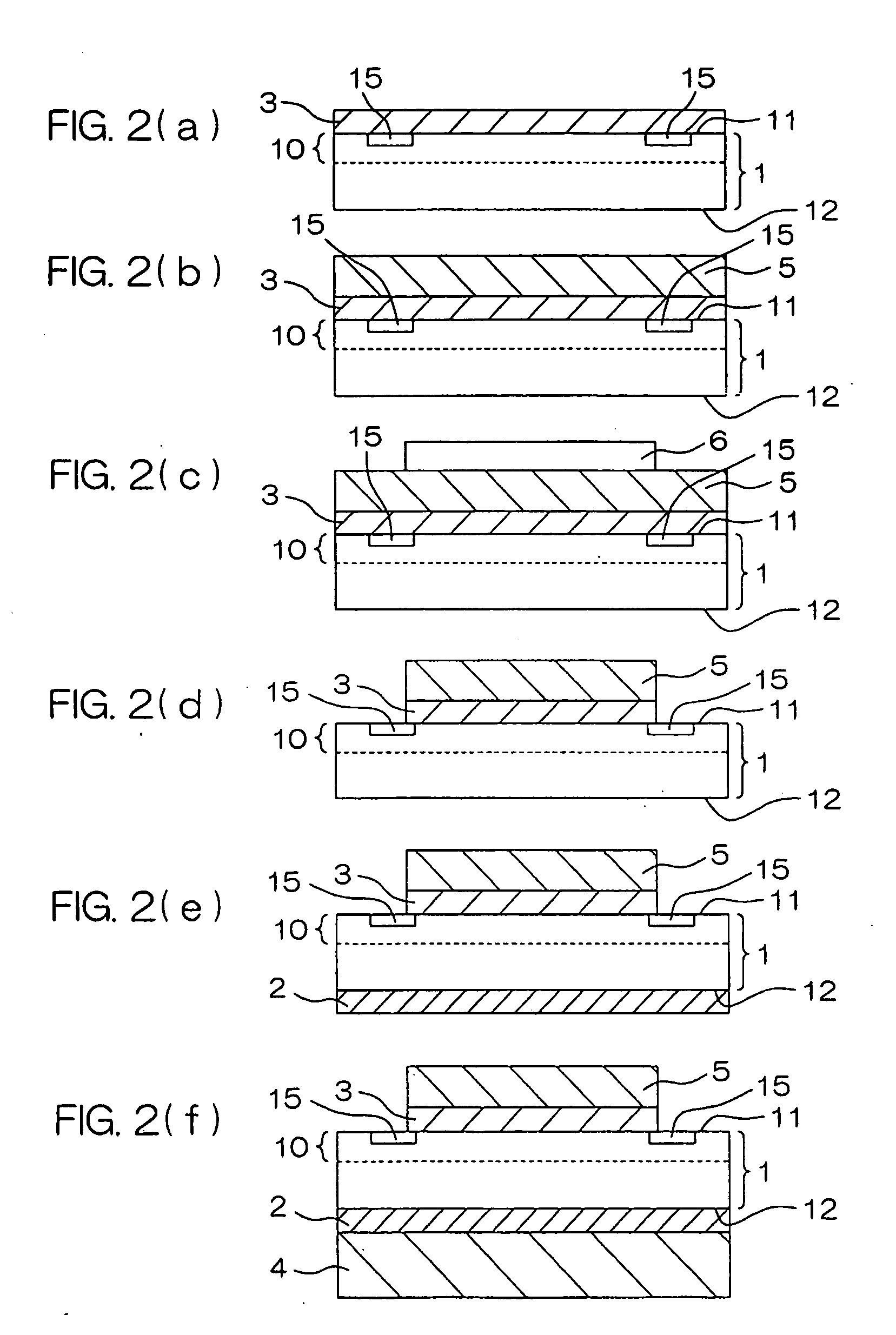

Image

  • Semiconductor device and method of manufacturing the same
  • Semiconductor device and method of manufacturing the same
  • Semiconductor device and method of manufacturing the same

Examples


Embodiment Construction

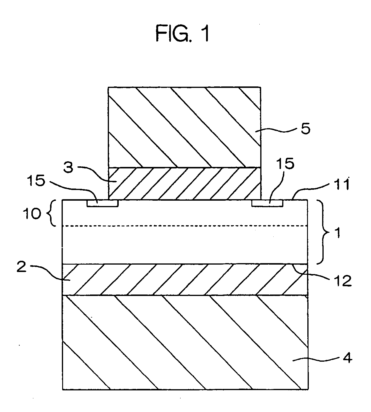
[0057]FIG. 1 is a cross-sectional view schematically showing the configuration of a semiconductor device according to an embodiment of the present invention. The semiconductor device is a Schottky barrier diode, for example. An example of a semiconductor substrate is an N-type SiC semiconductor substrate (e.g., a 4H—SiC epiwafer) 1 having a surface orientation of {0001} and having an off angle of 8°. An edge termination 15 is formed, in the SiC semiconductor substrate 1, by boron implantation and annealing at a relatively low temperature (approximately 1000° C.).

[0058] One surface of the SiC semiconductor substrate 1 is a silicon surface 11, and the other surface thereof is a carbon surface 12.

[0059] An N-type SiC semiconductor epitaxial layer 10 having a thickness of approximately 10 μm and having a carrier concentration of 4.0×10¹⁵ / cm3 to 8.0×10¹⁵ / cm3 is formed on the silicon surface 11. Consequently, the carrier concentration in the SiC semiconductor substrate 1 on the side of ...


PUM


Abstract

A semiconductor device provided with a silicon carbide semiconductor substrate, and an ohmic metal layer joined to one surface of the silicon carbide semiconductor substrate in an ohmic contact and composed of a metal material whose silicate formation free energy and carbide formation free energy respectively take negative values. The ohmic metal layer is composed of, for example, a metal material such as molybdenum, titanium, chromium, manganese, zirconium, tantalum, or tungsten.

Description

BACKGROUND OF THE INVENTION [0001] 1. Field of the Invention [0002] The present invention relates to a semiconductor device such as a Schottky barrier diode using a silicon carbide semiconductor substrate and a method of manufacturing the same. [0003] 2. Description of Related Art [0004] The configuration of a Schottky barrier diode using a silicon carbide (SiC) semiconductor substrate is as shown in FIG. 9(e). One surface of a SiC semiconductor substrate 100 is a silicon surface 110, and the other surface thereof is a carbon surface 120. A SiC epitaxial layer 101 is formed on the side of the silicon surface 110. [0005] A titanium (Ti) metal layer 30, for example, is formed on the silicon surface 110, and a Schottky junction is formed in an interface between the silicon surface 110 and the Ti metal layer 30. Further, an Al surface electrode 50, for example, is formed on a surface of the Ti metal layer 30 in order to ensure good adhesion to a metal wire composed of aluminum (Al) or t...

Claims


Application Information

Patent Timeline
IPC IPC(8): H01L21/04H01L29/24
CPCH01L29/1608H01L29/45H01L29/66143H01L29/6606H01L29/872H01L29/47H01L2224/05624H01L2224/05644H01L2224/05639H01L2224/05166H01L2224/0518H01L2224/45124H01L2224/73265H01L2224/32245H01L2924/10272H01L2224/04026H01L29/0615
Inventor OKAMURA, YUJIMATSUSHITA, MASASHI
Owner ROHM CO LTD
Learn More