Organic electroluminescent device

an electroluminescent device and organic technology, applied in the direction of discharge tube/lamp details, discharge tube luminescnet screens, other domestic articles, etc., can solve the problem that it is impossible to say that organic el devices having a sufficient efficiency and lifetime have been developed, and achieve the effect of improving the lifetime and reducing the device li

Active Publication Date: 2009-05-05
IDEMITSU KOSAN CO LTD
View PDF25 Cites 36 Cited by
  • Summary
  • Abstract
  • Description
  • Claims
  • Application Information

AI Technical Summary

Benefits of technology

[0011]The inventors have repeated investigations on the above-mentioned problems, so as to find out that: in an organic EL device as described above, carries (holes and electrons) which do not contribute to recombination pass through its organic emitting layer so as to be injected into charge-transporting layers at the reverse sides, so that the durability of the device lowers; and the lifetime of an organic EL device can be improved by causing a hole-trapping dopant and an electron-trapping dopant to be together present in its organic emitting layer. Thus, the invention has been made.
[0037]The lifetime and luminous efficiency of the organic electroluminescent device of the invention can be improved by making a hole-trapping dopant and an electron-trapping dopant to be present together in its organic emitting layer.

Problems solved by technology

However, it cannot be said that organic EL devices having a sufficient efficiency and lifetime have been developed.

Method used


Image

  • Organic electroluminescent device
  • Organic electroluminescent device
  • Organic electroluminescent device

Examples


first embodiment

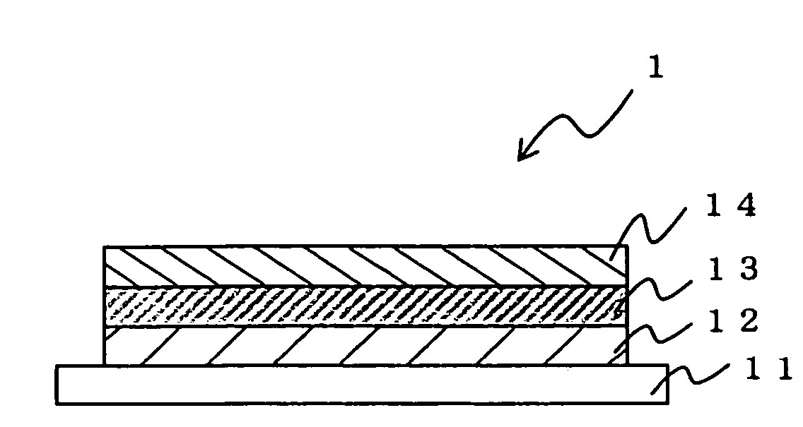
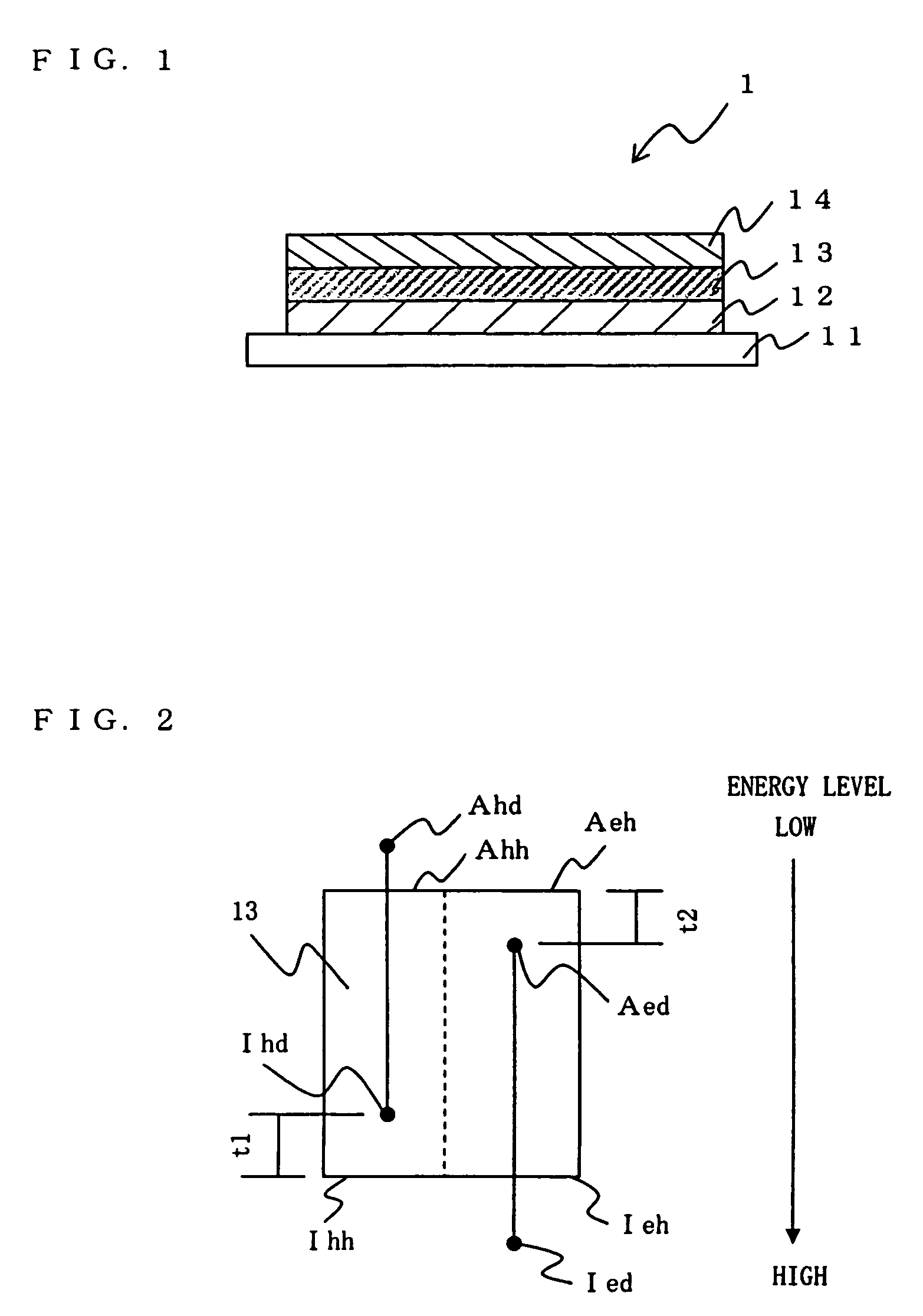
[0044]FIG. 1 is a schematic sectional view of an organic electroluminescent device which is a first embodiment of the invention.

[0045]The organic electroluminescent device 1 has a structure in which an anode 12, an organic emitting layer 13, and a cathode 14 are stacked, in this order, on a substrate 11. In this device, a voltage is applied thereto across the anode 12 and the cathode 14, whereby holes and electrons are injected from the anode 12 and the cathode 14, respectively, to the organic emitting layer 13. These are recombined in the organic emitting layer 13 to emit light.

[0046]In the embodiment, the organic emitting layer 13 is composed of a hole trapping dopant, an electron trapping dopant, a host material containing the hole trapping dopant, and a host material containing the electron trapping dopant.

[0047]FIG. 2 is an energy diagram of the organic electroluminescent device of the embodiment.

[0048]In this energy diagram are shown energy levels (ionization potentials and af...

second embodiment

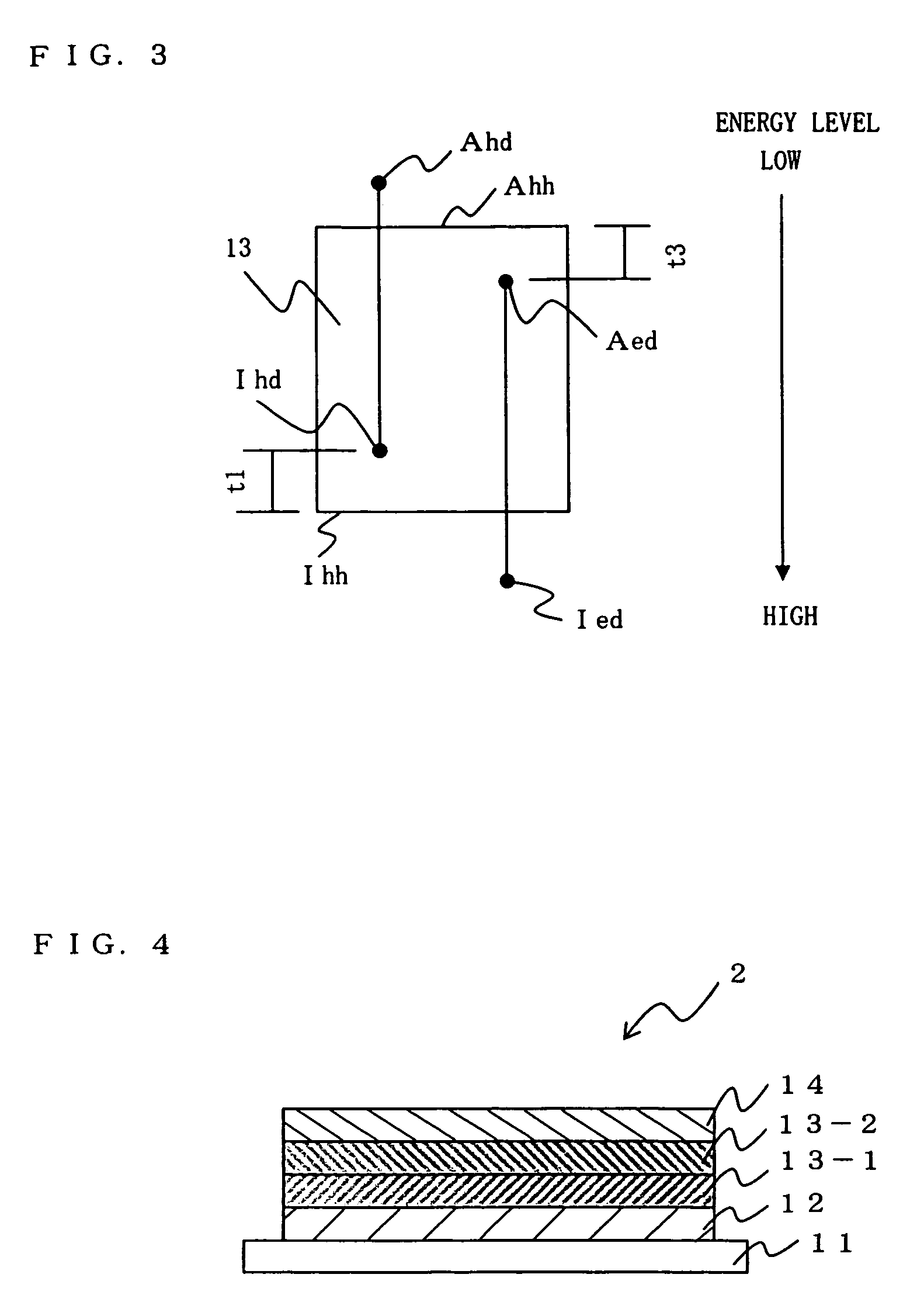
[0059]In the organic electroluminescent device of the invention, its organic emitting layer may have a stack structure.

[0060]FIG. 4 is a schematic sectional view of an organic electroluminescent device which is a second embodiment of the invention.

[0061]The organic electroluminescent device 2 has a structure wherein an anode 12, a first organic emitting layer 13-1, a second organic emitting layer 13-2 and a cathode 14 are stacked, in this order, on a substrate 11. When a voltage is applied to this device across the anode 12 and the cathode 14, holes and electrons are injected from the anode 12 and the cathode 14, respectively, to the first organic emitting layer 13-1 and the second organic emitting layer 13-2 so that these are recombined in the first and second organic emitting layers to emit light.

[0062]In the embodiment, the first organic emitting layer 13-1 is made of a first host material and a hole trapping dopant, and the second organic emitting layer 13-2 is made of a second ...

example 1

[0219]A glass substrate, 25 mm×75 mm×1.1 mm thick, having an ITO transparent electrode (manufactured by Geomatics Co.) was subjected to ultrasonic cleaning in isopropyl alcohol for 5 minutes followed by UV ozone cleaning for 30 minutes.

[0220]The cleaned glass substrate having transparent electrode lines was set up on a substrate holder in a vacuum deposition device. First, an N,N′-bis(N,N′-diphenyl-4-aminophenyl)-N,N-diphenyl-4,4′-diamino-1,1′-biphenyl film (abbreviated to “TPD 232 film” hereinafter) was formed in a thickness of 60 nm on the surface on which the transparent electrode lines were formed, so as to cover the transparent electrode. This TPD 232 film functioned as a hole-injecting layer.

[0221]After the formation of the TPD 232 film, a 20 nm thick N,N,N′,N′-tetra(4-biphenyl)-diaminobiphenylene layer (abbreviated to “TBDB layer” hereinafter) was formed on the TPD 232 film. This film functioned as a hole-transporting layer.

[0222]Furthermore, a 20 nm thick compound (H1) was d...


PUM


Abstract

An organic electroluminescent device 1 including: an anode 12, a cathode 14 and an organic emitting layer 13 held therebetween, the organic emitting layer 13 containing one or more host materials, a hole trapping dopant and an electron trapping dopant. The lifetime of an organic EL device 1 can be improved by causing a hole-trapping dopant and an electron-trapping dopant to be together present in its organic emitting layer.

Description

TECHNICAL FIELD[0001]The invention relates to an organic electroluminescent device.TECHNICAL BACKGROUND[0002]Organic electroluminescent devices, which may be referred to as organic EL devices, having an organic emitting layer have been promisingly expected to be used as large-area full-color display devices of a solid-state emitting type, and many developments thereof have been performed.[0003]Recently, practical use of organic EL device displays has been started, and thus the organic EL devices have been desired to have a higher luminance, a higher efficiency and a longer lifetime.[0004]A technique of incorporating a very small amount of a fluorescent molecule (dopant) into an organic emitting layer made mainly of a host material is known in order to meet the above-mentioned desires.[0005]There is also disclosed, for example, an organic EL device having an emitting layer including a mixture of a first component for accepting positive charge carriers (holes) from a first-charge-carr...

Claims


Application Information

Patent Timeline
Patent Type & Authority Patents(United States)
IPC IPC(8): H05B33/00
CPCH01L51/002H01L51/0054H01L51/0055H01L51/0056H01L51/5012H01L51/0058H01L51/0059H01L51/006H01L51/0081Y10S428/917H10K71/30H10K85/623H10K85/624H10K85/622H10K85/626H10K85/633H10K85/631H10K85/324H10K50/11C09K11/06
Inventor KAWAMURA, HISAYUKIKUBOTA, MINEYUKIFUNAHASHI, MASAKAZU
Owner IDEMITSU KOSAN CO LTD
Why Eureka
Try Eureka