Programmable read-only memory

a read-only memory and programmable technology, applied in the field of programmable read-only memory, can solve the problems of increasing the cost of manufacturing such a memory, limiting the number of memory cells, and not always being a standard process feature, so as to reduce the area, reduce the cost of production or manufacturing yield, and the effect of increasing capacity

Active Publication Date: 2009-05-05
III HLDG 12 LLC
View PDF19 Cites 6 Cited by
  • Summary
  • Abstract
  • Description
  • Claims
  • Application Information

AI Technical Summary

Benefits of technology

[0031]It is thus possible to provide a memory in which the or each memory cell comprises a transistor which also forms a fusible element. The area occupied by such a cell may therefore be substantially smaller than for cells of known types. Row and column logic circuits may operate at nominal supply voltages during the programming step and it is possible, in some embodiments, for a global programming voltage to be applied to all cells simultaneously. Relatively large devices for passing relatively large currents during programming may therefore be eliminated or substantially reduced in number so that the area occupied by the memory may be substantially less than for known types of memories. No additional processing steps are necessary during manufacture of such a memory. It is therefore possible to provide a memory of reduced area and / or higher capacity with little or no penalty in cost of production or in manufacturing yield.

Problems solved by technology

This in turn means that a relatively large area of an integrated circuit forming the memory is required and limits the number of memory cells which may be integrated in a given area of the memory device.
However, such thin oxides are not always a standard process feature of the manufacturing process for making such memories.
Additional processing steps may therefore be necessary and this increases the cost of manufacture of such a memory and may reduce the manufacturing yield.
However, in a typical low temperature poly-silicon TFT process, the provision of such a structure would require additional process steps.

Method used


Image

  • Programmable read-only memory
  • Programmable read-only memory
  • Programmable read-only memory

Examples


Embodiment Construction

[0057]Like reference numerals refer to like parts throughout the drawings.

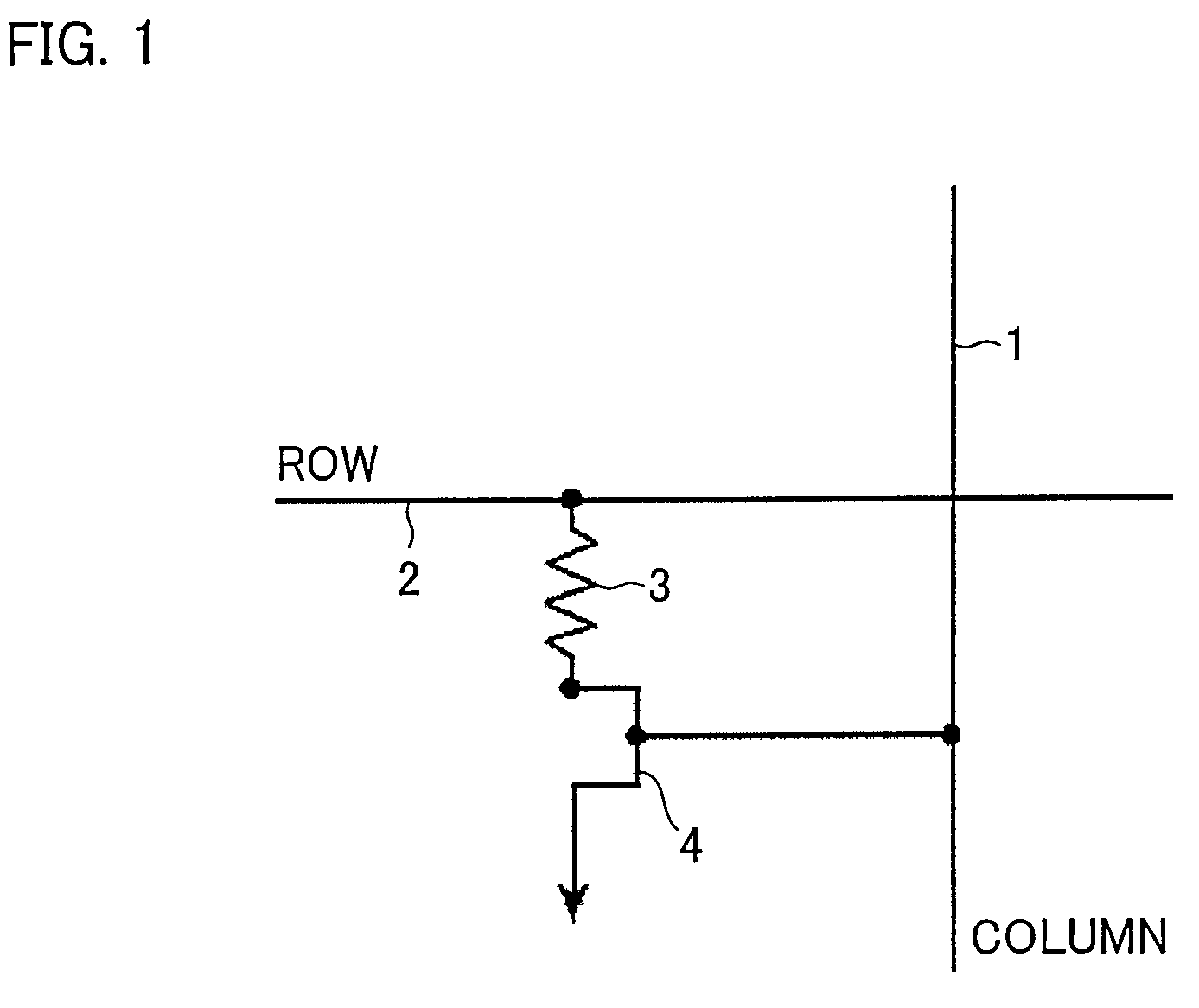
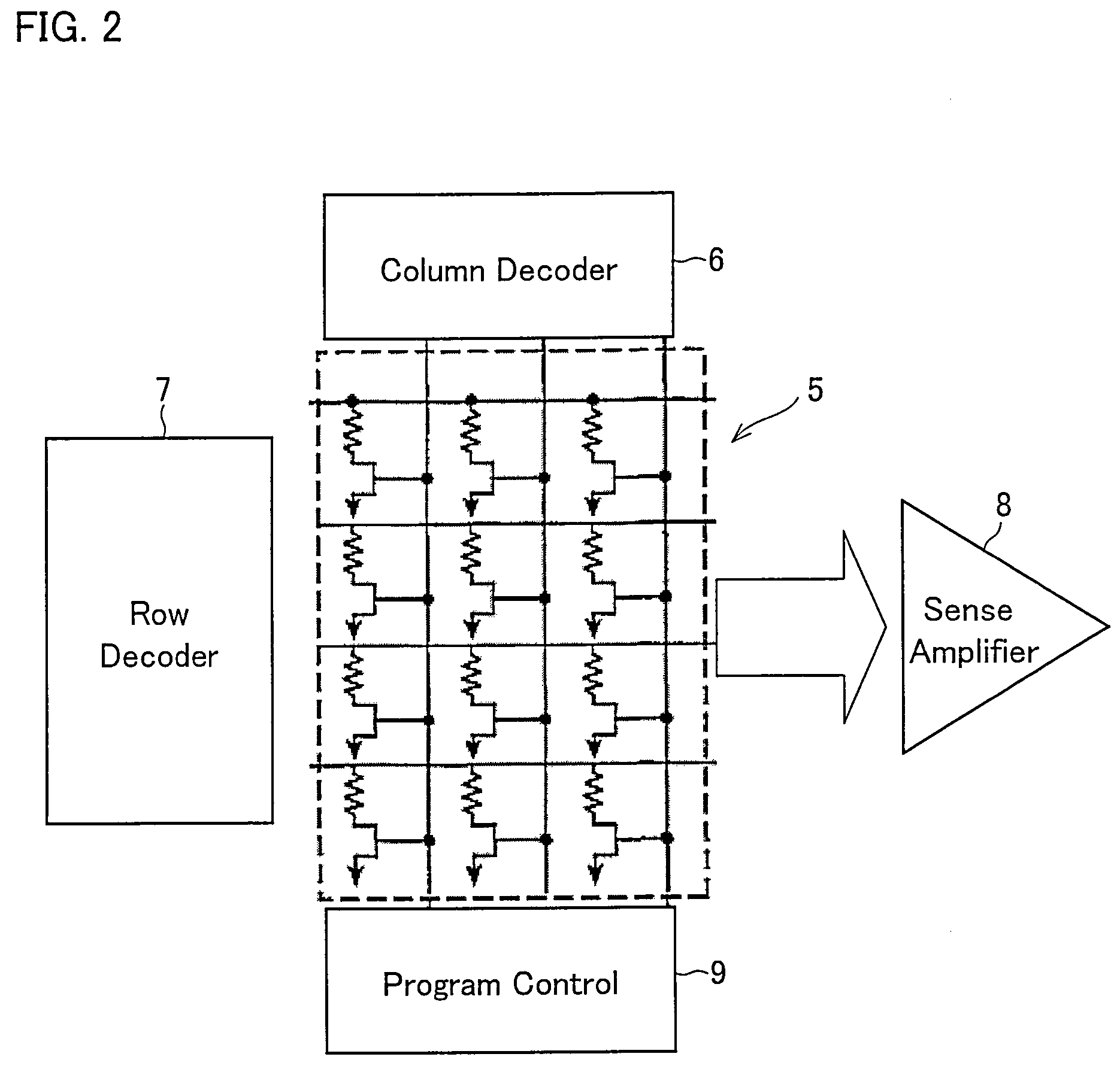
[0058]The memory cell shown in FIG. 8 may be used as a single bit PROM for non-volatile storing of a single bit of information. More typically, the memory cell is used as one element of an array of memory cells which, together with row and column decoding circuits and read and programming circuits, forms a memory for storing multiple bits or multiple words of information. Such a memory may be formed as an integrated circuit for use with other devices or circuits or may form part of an integrated circuit incorporating circuitry for performing other functions.

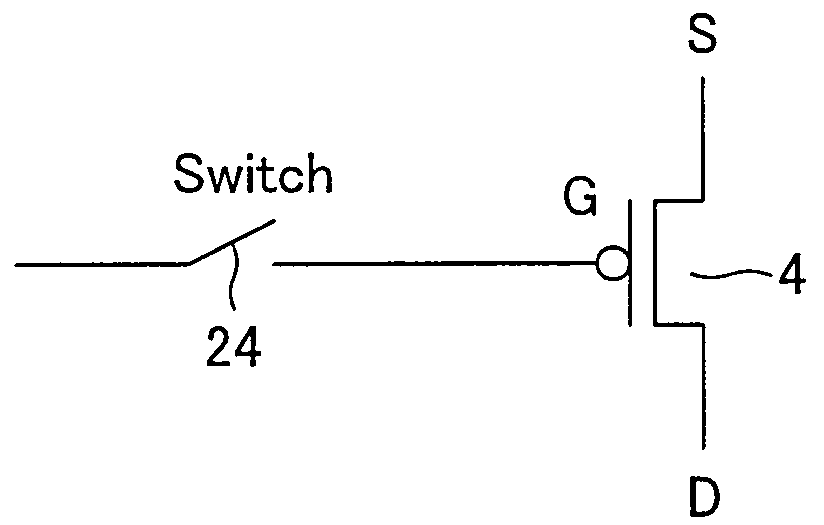
[0059]The memory cell comprises a transistor 4 and an electronic switch (first electronic switch) 24. In the example shown in the FIG. 8, the transistor 4 is an insulated gate field effect transistor (IGFET), for example formed as a metal oxide silicon (MOS) transistor. For example, the transistor may be a thin film transistor (TFT) and has a control electr...


PUM


Abstract

A programmable read-only memory comprises a memory cell or a plurality of such cells arranged as an array. Each memory cell comprises a transistor, such as a MOS TFT. An electronic switch allows the control electrode, such as the gate, to be substantially electrically isolated during a programming mode so that the gate is electrically floating during this mode. During the programming mode, a programming voltage is supplied across the main conductive path of the transistor, such as across the source-drain channel. The programming voltage is sufficiently large to fuse the main conduction path when the control electrode of the transistor is floating but is insufficient to fuse the main conduction path when the control electrode is not floating and is connected to a suitable defined voltage. The transistor therefore performs functions of memory cell selection while simultaneously acting as the fusible element and the arrangement requires fewer transistors which are capable of operating at the programming current required for fusing. The memory may therefore occupy a reduced area.

Description

[0001]This Nonprovisional application claims priority under 35 U.S.C. § 119(a) on Patent Application No. 0607482.7 filed in U.K. on Apr. 13, 2006, the entire contents of which are hereby incorporated by reference.FIELD OF THE INVENTION[0002]The present invention relates to a programmable read-only memory. Such a memory may be used as a non-volatile memory for or in an integrated circuit, for example in applications which require storage of non-volatile “write-once” data. Examples of such applications include system identity data and post-production calibration data.BACKGROUND OF THE INVENTION[0003]Write-once or “one-time” programmable memory cells have been used in programmable read-only memory (PROM) arrays for many years. Two types of memory cells are in use and are known as “fuse” and “anti-fuse” types.[0004]FIG. 1 of the accompanying drawings illustrates a known type of memory cell forming part of an array addressed by column electrodes such as 1 and row electrodes such as 2. Ea...

Claims


Application Information

Patent Timeline
Patent Type & Authority Patents(United States)
IPC IPC(8): G11C7/00
CPCG11C17/16G11C2216/26G11C17/08G11C17/10G11C17/12
Inventor SHAH, SUNAYABED-MERAIM, OLIVIER KARIMZEBEDEE, PATRICK
Owner III HLDG 12 LLC
Why Eureka
Try Eureka