Semiconductor device

a technology of semiconductor devices and dielectric constants, applied in semiconductor devices, semiconductor/solid-state device details, electrical apparatus, etc., can solve the problem that the technique does not necessarily provide the higher level of adhesiveness, and achieve the effect of improving the adhesiveness of the interior, reducing the dielectric constant, and improving the adhesiveness between

Inactive Publication Date: 2009-05-12
RENESAS ELECTRONICS CORP
View PDF17 Cites 21 Cited by
  • Summary
  • Abstract
  • Description
  • Claims
  • Application Information

AI Technical Summary

Benefits of technology

[0009]In view of the above situation, the present invention provides a solution to the above-mentioned problems, and the present invention provides a technology to improve the interlayer adhesiveness of the interlayer insulating film layer.
[0010]Conventionally, a technique for improving the adhesiveness at an interface of films of different types, which has been investigated, is to design a preferable component of the films by suitably selecting the materials of the films. However, this technique does not necessarily easily provide the higher level of the adhesiveness that is expected in recent years. The inventors of the present invention has considered that a thermal stress is remained at the interface of the films by a thermal history undertaken in the semiconductor manufacturing process, and the thermal stress induces the decrease of the adhesiveness, and on the basis of the consideration, a solution to the above-described problem is achieved. As a result of eagerly conducting the investigations in view of the aforementioned consideration, the inventors of the present invention have found that suitable design of the interlayer insulating film by focusing an attention to the film density is effective for improving the adhesiveness at the interface, and thus the present invention is made on the basis of such finding.
[0012]The semiconductor device according to the present invention has a configuration, which comprises the first density transition region having the film density distribution profile, in which the film density gradually decreases as a distance from the first insulating film increases. Thus, the interlayer insulating film having improved adhesiveness of the interior of the multilayered film can be presented, while providing a lower dielectric constant. As above-described, having such a film density distribution, in which the film density gradually decreases as the distance increases from the first insulating film, stress generated at the interface between the first insulating film and the second insulating film is gradually relaxed, thereby considerably improving the adhesiveness therebetween. This improvement, in turn, provides improved thermal cycle resistance, and thus the semiconductor device having higher reliability can be achieved. Although a specific limitation is laid on the design of the dielectric constant of the second insulating film in the side having the first insulating film provided thereon, due to the presence of the density transition region having above-described configuration, the dielectric constant of the whole second insulating film can be reduced, since the dielectric constant of the other region thereof can be arbitrarily selected to a lower value.
[0013]According to the present invention, since the device has multilayered film having a film density distribution, in which the film density gradually decreases in the interlayer insulating films, the adhesiveness between films that composes the interlayer insulating film can be improved.

Problems solved by technology

However, this technique does not necessarily easily provide the higher level of the adhesiveness that is expected in recent years.

Method used


Image

  • Semiconductor device
  • Semiconductor device
  • Semiconductor device

Examples


first embodiment

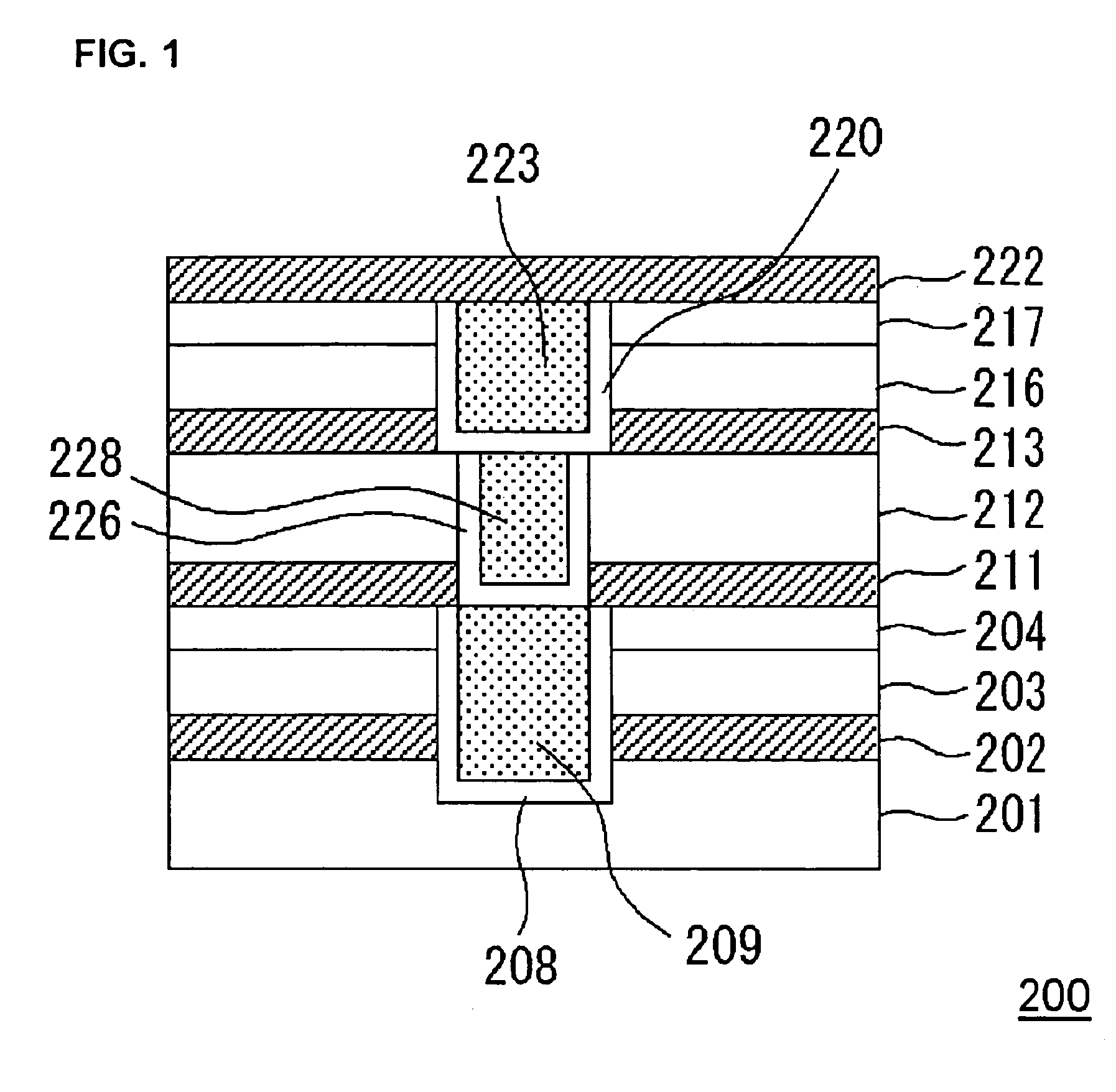
[0028]FIG. 1 is a cross-sectional view, showing a structure of a semiconductor device 200 according to the present embodiment. The semiconductor device 200 according to the present embodiment has a structure, in which an interlayer insulating film is formed on a silicon substrate, and a multilayered interconnect structure comprising copper interconnects and vias is provided within the interlayer insulating film. The illustrated structure is an example showing a portion of such multilayered interconnect structure, and the structure has a configuration, in which a lower layer interconnect consisting of a Cu film 209 is coupled to an upper layer interconnect consisting of a Cu film 223 via a copper plug 228.

[0029]The lower layer interconnect consisting of the Cu film 209 is formed within a multilayered film comprising an underlying insulating film 201, a SiCN film 202 that is a first insulating film, a SiOC film 203 that is the second insulating film and a SiO2 film 204 that is a third...

second embodiment

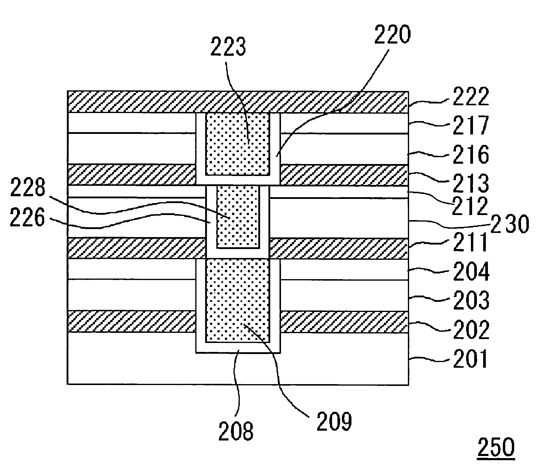
[0046]FIG. 3 is a cross-sectional view, showing a structure of a semiconductor device 250 according to the present embodiment. The semiconductor device 250 according to the present embodiment has a structure, in which an interlayer insulating film is formed on a silicon substrate, and a multilayered interconnect structure comprising copper interconnects and vias is provided within the interlayer insulating film. The illustrated structure is an example showing a portion of such multilayered interconnect structure, and the structure has a configuration, in which a lower layer interconnect consisting of a Cu film 209 is coupled to an upper layer interconnect consisting of a Cu film 223 via a copper plug 228.

[0047]The copper plug 228 is provided in a via hole, which is formed in a multilayered film composed of a SiCN film 211 that is a first insulating film, a SiOC film 230 that is the second insulating film and a SiO2 film 212 that is a third insulating film, and the side surfaces and ...

third embodiment

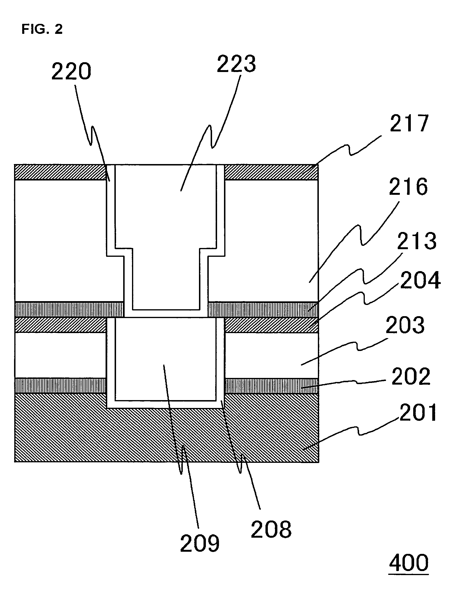
[0060]In the present embodiment, an example illustrating a method of manufacturing a semiconductor device shown in the first embodiment will be described. Description will be made in reference with FIGS. 4A to 4D.

[0061]First of all, a structure shown in FIG. 4A is produced. First, an underlying insulating film 201 is provided on a substrate (not shown in the drawings), which has a semiconductor device formed thereon, and a SiCN film 202 for functioning as an etch stopper film in a process for forming an interconnect trench is deposited thereon to a thickness of 50 nm via a plasma CVD process.

[0062]Then, the SiOC film 203 is deposited to a thickness of 300 nm via a plasma CVD process, in which a flow rate of trimethylsilane gas is stepwise increased. In this case, the film density of the deposited SiOC film 203 is gradually decreased by stepwise increasing the flow rate of trimethylsilane gas. Since trimethylsilane contains methyl group, trimethylsilane has more bulky molecular struc...


PUM


Abstract

A semiconductor device having improved adhesiveness between films composing an interlayer insulating film is presented by providing multilayered films in the interlayer insulating films having film density distribution, in which the film density is gradually changes. A SiOC film is deposited to a thickness of 300 nm via a plasma CVD process, in which a flow rate of trimethylsilane gas is stepwise increased. In this case, the film density of the deposited SiOC film is gradually decreased by stepwise increasing the flow rate of trimethylsilane gas. Since trimethylsilane contains methyl group, trimethylsilane has more bulky molecular structure in comparison with monosilane or the like. Thus, the film density is decreased by increasing the amount of trimethylsilane in the reactant gas.

Description

[0001]This application is based on Japanese Patent Application NO. 2004-027158, the content of which is incorporated hereinto by reference.BACKGROUND OF THE INVENTION[0002]1. Field of the Invention[0003]The present invention relates to a semiconductor device having an improved interlayer adhesiveness in an interlayer insulating film.[0004]2. Related Art[0005]Needs for achieving faster operation of semiconductor devices are growing in recent years, and in order to meet the needs, technologies for providing a metal interconnect with copper to reduce the interconnect resistance are widely employed. Such interconnect structure is formed via a damascene process including a chemical mechanical polishing (CMP) process.[0006]When a damascene copper interconnect is formed, it is essential to provide an etch stopper film for forming an interconnect trench and / or a through hole, or a protective film for inhibiting the damage to the interlayer insulating film occurred during the chemical mechan...

Claims


Application Information

Patent Timeline
Patent Type & Authority Patents(United States)
IPC IPC(8): H01L23/58H01L21/31H01L29/00H01L23/522H01L21/316H01L21/768H01L23/48H01L23/532
CPCH01L21/76801H01L23/53295H01L23/53233H01L23/53238Y10S438/931H01L2924/0002H01L2924/00
Inventor OHTO, KOICHIUSAMI, TATSUYASASAKI, YOICHI
Owner RENESAS ELECTRONICS CORP
Why Eureka
Try Eureka