Q-boosting circuit

a boosting circuit and circuit technology, applied in the direction of electric variable regulation, process and machine control, instruments, etc., can solve the problems of limited improvement range of q factor and significant deterioration of q factor of inductor, so as to reduce a resistance component of the transformer and improve q factor

Inactive Publication Date: 2009-05-12
ELECTRONICS & TELECOMM RES INST
View PDF14 Cites 14 Cited by
  • Summary
  • Abstract
  • Description
  • Claims
  • Application Information

AI Technical Summary

Benefits of technology

[0016]It is an object of the present invention to provide a Q-boosting circuit that reduces an equivalent resistance component of a transformer using a negative resistance circuit (e.g., negative conductance (gm) circuit) and thereby solves drawbacks described above.
[0020]The present invention is applied to a radio frequency (RF) integrated circuit using a transformer instead of an inductor in a semiconductor device such as a complementary metal oxide semiconductor (CMOS). The present invention couples a negative resistance circuit to one pair of terminals of a transformer having at least three pairs of terminals, thereby reducing a resistance component of the transformer. Therefore, it is possible to obtain a more improved Q factor than a conventional Q factor through adjustment of a mutual inductance component and a resistance component and obtain the Q factor having a wide range from several tens to several hundreds according to a frequency range.

Problems solved by technology

When an inductor is integrated, the Q factor of the inductor considerably deteriorates.
That is, an improvement range of the Q factor is limited.

Method used


Image

  • Q-boosting circuit
  • Q-boosting circuit
  • Q-boosting circuit

Examples


Embodiment Construction

[0029]Hereinafter, an exemplary embodiment of the present invention will be described in detail. However, the present invention is not limited to the embodiments disclosed below, but can be implemented in various types. Therefore, the present embodiment is provided for complete disclosure of the present invention and to fully inform the scope of the present invention to those ordinarily skilled in the art.

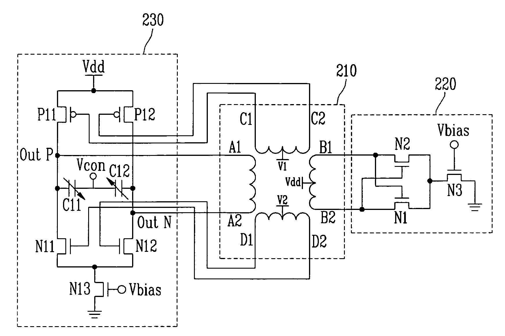
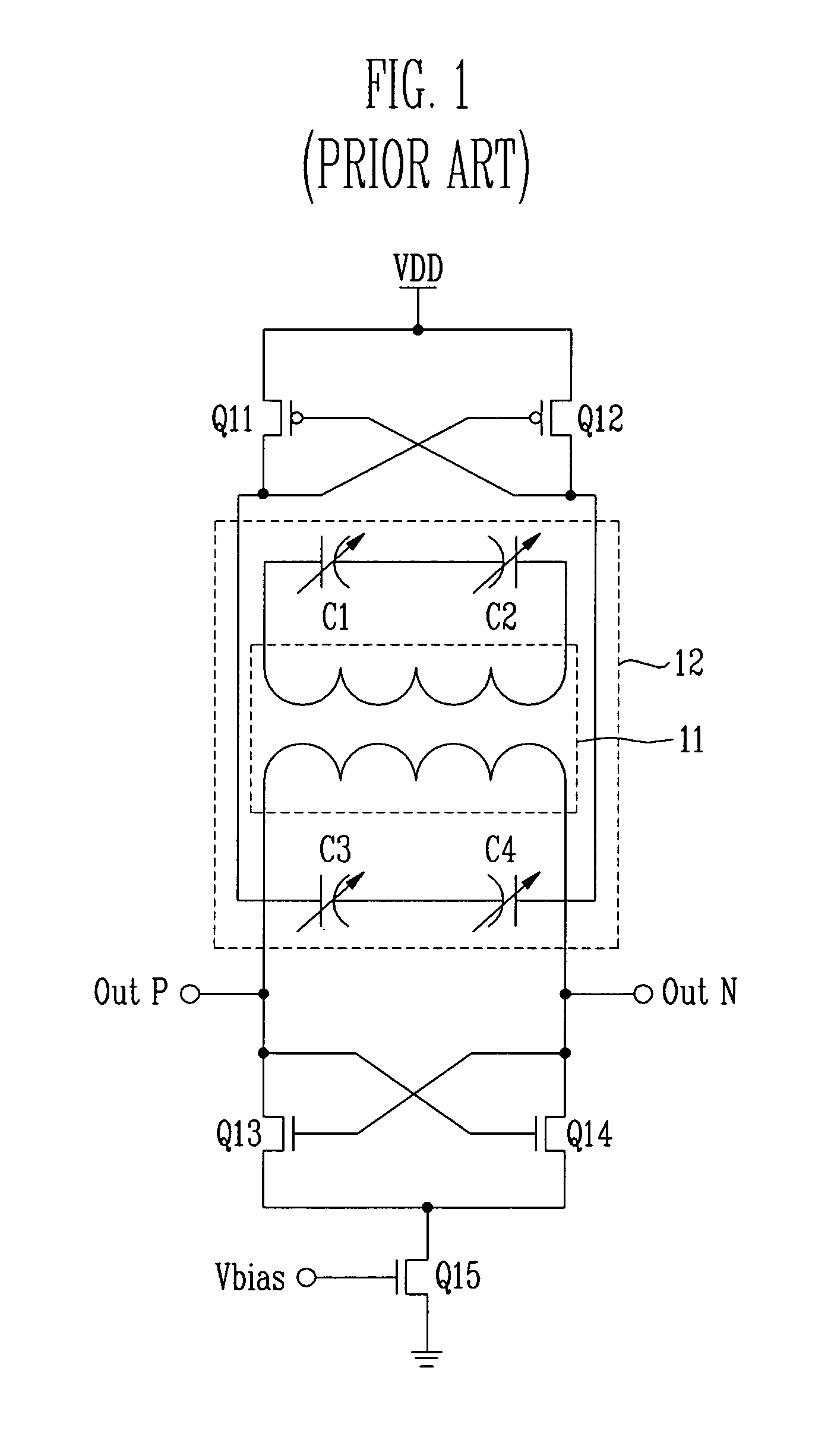
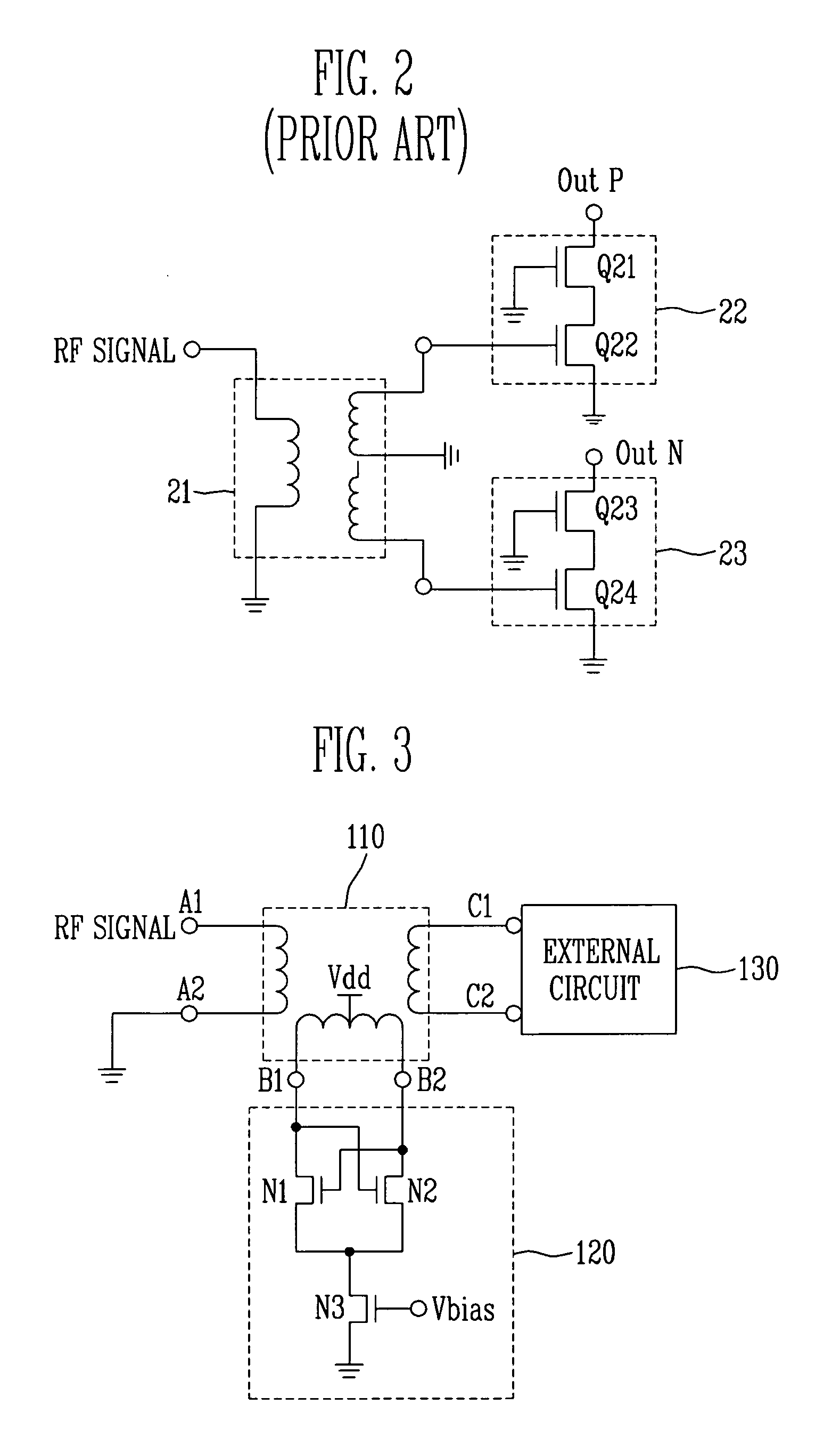
[0030]FIG. 3 is a circuit diagram illustrating a Q-boosting circuit according to an exemplary embodiment of the present invention. The Q-boosting circuit comprises a transformer 110 for providing a predetermined inductance L, and a negative resistance circuit 120 for reducing a resistance component of the transformer 10.

[0031]The transformer 10 includes at least three pairs of terminals A1 and A2, B1 and B2, and C1 and C2, and provides the predetermined inductance L according to numbers of winds of coils each coupled between the terminals A1 and A2, B1 and B2, and C1 and C2. A plan...


PUM


Abstract

Provided is a Q-boosting circuit for improving a Q factor in a radio frequency (RF) integrated circuit of a semiconductor device using a transformer instead of an inductor. The Q-boosting circuit couples a negative resistance circuit to a pair of terminals of a transformer to reduce a resistance component of the transformer, thereby increasing a mutual inductance component. Therefore, it is possible to obtain a more improved Q factor than a conventional Q factor through adjustment of an inductance and a resistance component, and to obtain the Q factor having a wide range from several tens to several hundreds according to a frequency range.

Description

CROSS-REFERENCE TO RELATED APPLICATION[0001]This application claims priority to and the benefit of Korean Patent Application No. 2005-89713, filed Sep. 27, 2005, the disclosure of which is incorporated herein by reference in its entirety.BACKGROUND[0002]1. Field of the Invention[0003]The present invention relates to a radio frequency (RF) integrated circuit of a semiconductor device using a transformer instead of an inductor, and more particularly, to a Q-boosting circuit capable of enhancing a quality factor (Q).[0004]2. Discussion of Related Art[0005]Recently, as a mobile communication service is expanding fast and the size of a terminal is reduced, it is required to reduce the size of an inductance-capacitance (LC) resonator, used in an RF integrated circuit such as a voltage-controlled oscillator (VCO).[0006]When an inductor is integrated, the Q factor of the inductor considerably deteriorates. Thus, in order to solve this problem, a method that embodies an inductor using a tran...

Claims


Application Information

Patent Timeline
Patent Type & Authority Patents(United States)
IPC IPC(8): G01R33/00
CPCH03B5/1228H03B5/1212H03B5/1296H03B5/124H03B5/08H03B5/02
Inventor LEE, YOUNG JAEYU, HYUN KYU
Owner ELECTRONICS & TELECOMM RES INST
Why Eureka
Try Eureka