Semiconductor device

a technology of semiconductors and devices, applied in the direction of semiconductor devices, electrical devices, transistors, etc., can solve the problems of uneven current densities of chips, narrow safe operating area, and risk of thermal runaway, so as to increase resistance components and increase current densities. uneven

Active Publication Date: 2011-08-23
SEMICON COMPONENTS IND LLC
View PDF8 Cites 0 Cited by
  • Summary
  • Abstract
  • Description
  • Claims
  • Application Information

AI Technical Summary

Benefits of technology

[0013]Thus, a problem arises that collector currents are likely to concentrate on the current path CP1′, thereby making current densities of a chip uneven. The uneven current densities increase a risk of thermal runaway, which will cause a problem of narrowing an area of safe operating (herein after referred to as ASO). In addition, another problem arises that generation of cells which do not operate when power is ON further increases resistance components, thus increasing unevenness of the current densities.

Problems solved by technology

Thus, a problem arises that collector currents are likely to concentrate on the current path CP1′, thereby making current densities of a chip uneven.
The uneven current densities increase a risk of thermal runaway, which will cause a problem of narrowing an area of safe operating (herein after referred to as ASO).
In addition, another problem arises that generation of cells which do not operate when power is ON further increases resistance components, thus increasing unevenness of the current densities.

Method used


Image

  • Semiconductor device
  • Semiconductor device
  • Semiconductor device

Examples


first embodiment

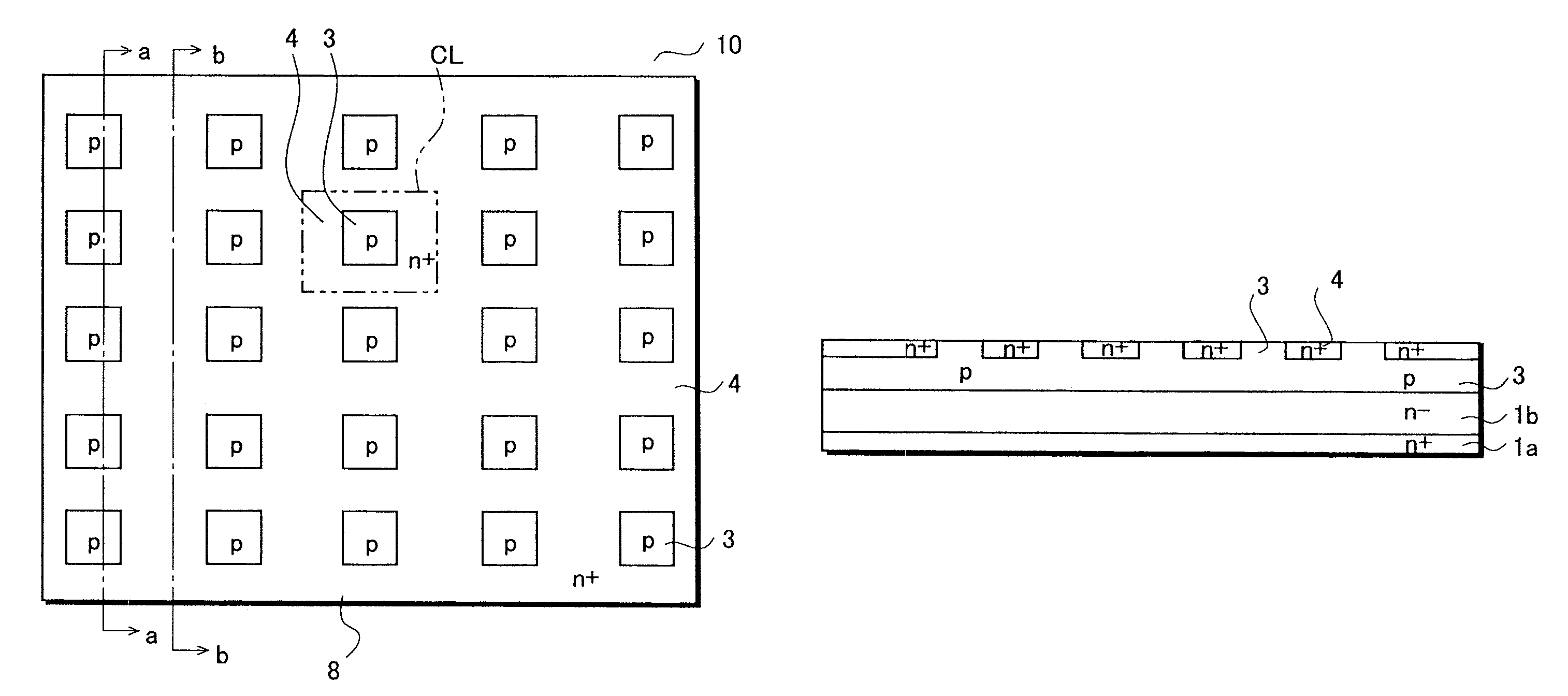
[0022]FIGS. 1A to 1C are views showing a structure of the semiconductor device 10, which is a FIGS. 1A to 1C show an operating region. FIG. 1A is a plan view. FIG. 1B is a cross sectional view taken along the line a-a of FIG. 1A. FIG. 1C is a cross sectional view taken along the line b-b of FIG. 1A.

[0023]A semiconductor substrate 1 is formed with an n+ type semiconductor substrate 1a of high concentration having an n− type semiconductor layer 1b provided thereon by epitaxial growth, for example. The semiconductor substrate 1 serves as a collector region of a bipolar transistor.

[0024]A base region 3 is a p-type diffusion region provided on a surface of the collector region. On a surface of the base region 3, an emitter region 4 is formed by diffusing n+ type impurities in a lattice pattern. With this, the base region 3 is separated into islands which are shown in squares in FIG. 1A. Here, the base region has its surface portion separated into islands, and a deep region which is form...

second embodiment

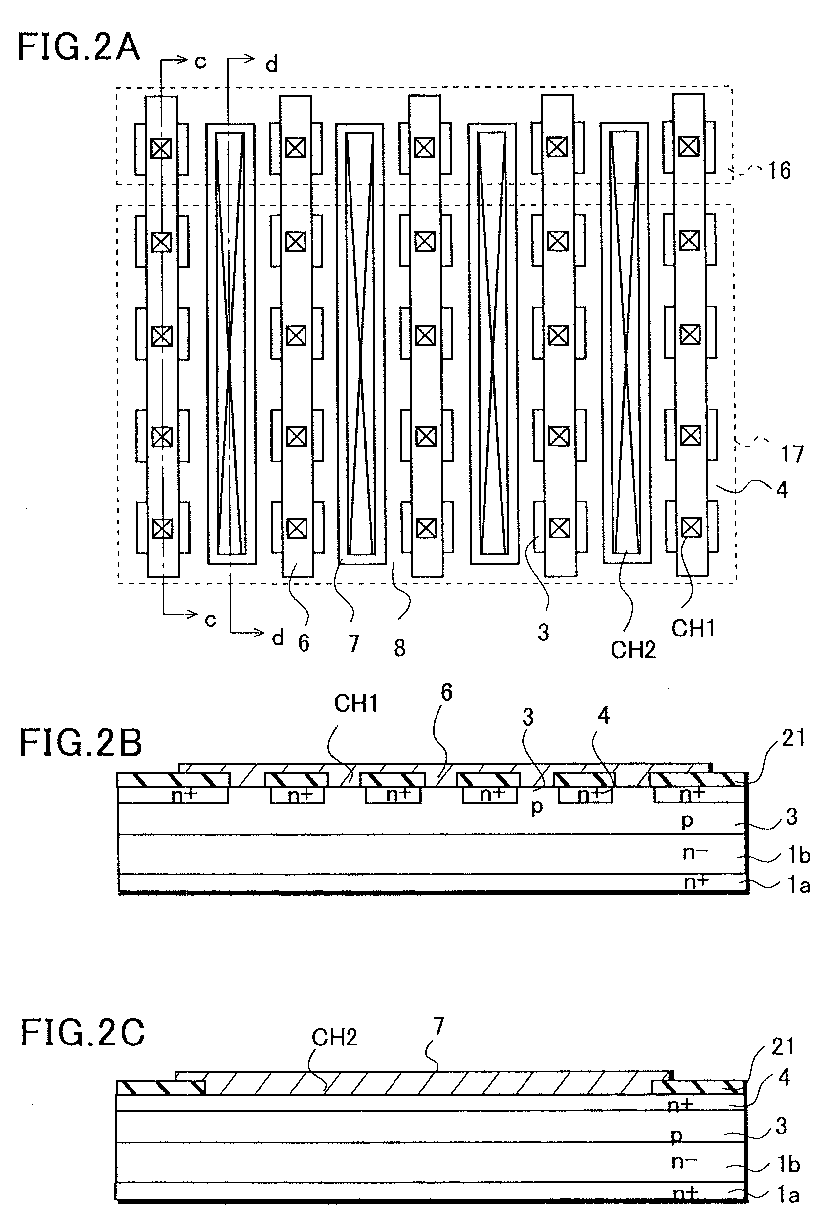
[0046]With reference to FIGS. 4A and 4B and FIGS. 5A to 5C, a description will be given of an example of the semiconductor device 10 described above. FIGS. 4A and 4B are plan views showing a second base electrode 16 and a second emitter electrode 17 of the semiconductor device 10. FIG. 4A is a plan view showing both electrode layers and a part of configuration of the lower layers. FIG. 4B is a plan view illustrating the second base electrode 16, the second emitter electrode 17, and an external connection connected thereto.

[0047]In the second embodiment, the second base electrode 16 and the second emitter electrode 17 are respectively patterned either into a concavo or convex shape, and are arranged so that concave portion engage with convex portion. A configuration here is similar to that of the first embodiment except for the pattern of the second base electrode 16, the pattern of the second emitter electrode 17, and the external connection connected to the second emitter electrode...


PUM


Abstract

The first base electrodes and the first emitter electrodes are all formed like strips, and are alternately arranged in parallel, and the area of the second emitter electrode is expanded to be larger than that of the second base electrode. With this, the number of current paths increases in each of which a current is pulled up almost straight from the emitter region to the second emitter electrode through the first emitter electrodes, thereby preventing the current densities of the entire chip from becoming uneven.

Description

[0001]This application claims priority from Japanese Patent Application Number JP 2008-217104 filed on Aug. 26, 2008, and Japanese Patent Application Number JP 2009-166992 filed on Jul. 15, 2009, the contents of which are incorporated herein by reference in their entirety.BACKGROUND OF THE INVENTION[0002]1. Field of the Invention[0003]The present invention relates to a semiconductor device, and more specifically to a semiconductor device capable of expanding an area of safe operating, avoiding thermal runaway, and achieving a reduction of resistance components, in a transistor.[0004]2. Description of the Related Art[0005]As a bipolar transistor of a discrete type, known is a bipolar transistor in which base electrodes are arranged in two layers and emitter electrodes are arranged in two layers, on an operating region formed of a lattice-patterned emitter region and an island-shaped base region (this technology is described for instance in Japanese Patent Application Publication No. ...

Claims


Application Information

Patent Timeline
Patent Type & Authority Patents(United States)
IPC IPC(8): H01L29/73
CPCH01L29/41708H01L24/34H01L29/732H01L29/73H01L24/06H01L2224/48247H01L2224/48465H01L2224/49107H01L2224/73221H01L2224/73265H01L2224/0603H01L2924/1305H01L2224/48463H01L2224/32245H01L2924/00H01L2224/02166H01L2224/04042H01L2224/37599H01L2224/37147H01L2224/33181H01L2924/00014H01L2924/00012H01L24/37
Inventor TAKAHASHI, KAZUYA
Owner SEMICON COMPONENTS IND LLC
Why Eureka
Try Eureka