
Monolithically integrated vertical pin photodiode used in biCMOS technology

a technology of monolithic integration and photodiodes, applied in semiconductor devices, basic electric elements, electric devices, etc., can solve problems such as contributing to process production costs, and achieve the effect of increasing the effort involved in the manufacturing process and enhancing the formation of a vertical integrated photodiodes

Active Publication Date: 2009-05-19
X FAB SEMICON FOUNDRIES
View PDF9 Cites 7 Cited by
  • Summary
  • Abstract
  • Description
  • Claims
  • Application Information

AI Technical Summary

Benefits of technology

The present invention provides an improvement to the operating speed and efficiency of a vertical integrated photodiode in biCMOS technology without significantly increasing manufacturing costs. This is achieved by using a combination of a p− epitaxial layer and a doped n− epitaxial layer, with lateral bordering by p well regions and buried p layers. The invention also includes an anode terminal on the bottom side of the substrate and an optional backside contact on the bottom side of the substrate, which can be thinned. The invention can be used in OEICs based on biCMOS technology to extend their applications.

Problems solved by technology

With PIN photodiodes monolithically integrated into silicon chips, however, the problem to be solved is that the dopant concentration of the substrate ranges from 1015 cm−3 and even higher for CMOS wells and n-collectors / epitaxial layers of npn transistors formed in bipolar and biCMOS technology.
For this purpose, at least three additional masking steps are necessary, thereby significantly contributing to production costs of the process.

Method used


Image

  • Monolithically integrated vertical pin photodiode used in biCMOS technology
  • Monolithically integrated vertical pin photodiode used in biCMOS technology
  • Monolithically integrated vertical pin photodiode used in biCMOS technology

Examples


Embodiment Construction

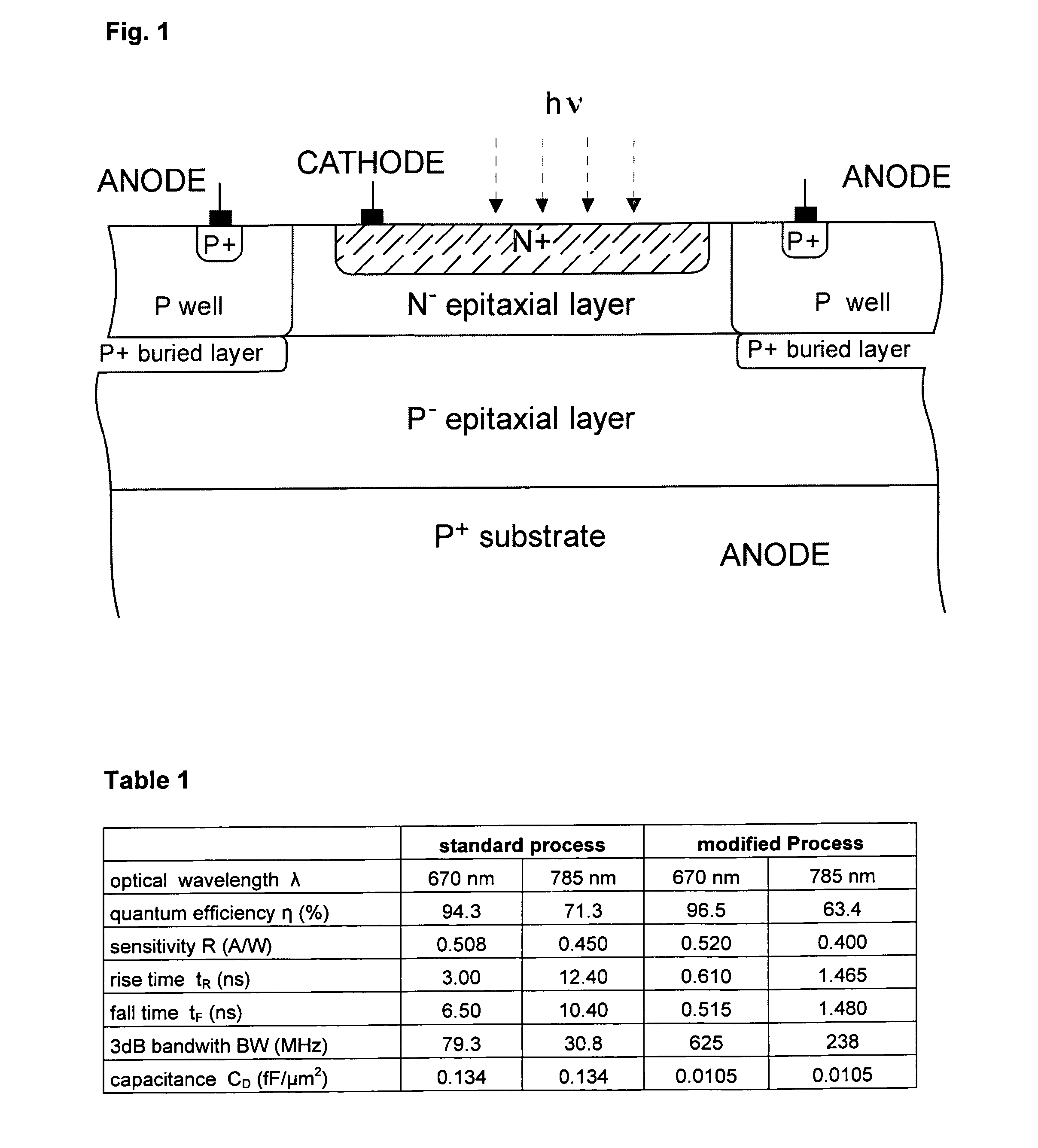
[0019]Table 1 includes the measurement results of photodiodes implemented by a non-modified and a modified biCMOS process, respectively. It is evident that according to the modification of the present invention for a wavelength of 670 nm, an integrated photodiode having a quantum efficiency of more than 95% may be obtained, wherein the short rise and fall times allow a processing bit rate of up to 1 Gbit / second. A reduced junction capacity CD allows for an increased photodiode area, which represents a further advantage.

[0020]FIG. 1 illustrates the exemplary embodiment of a monolithically vertical PIN diode formed in biCMOS technology.

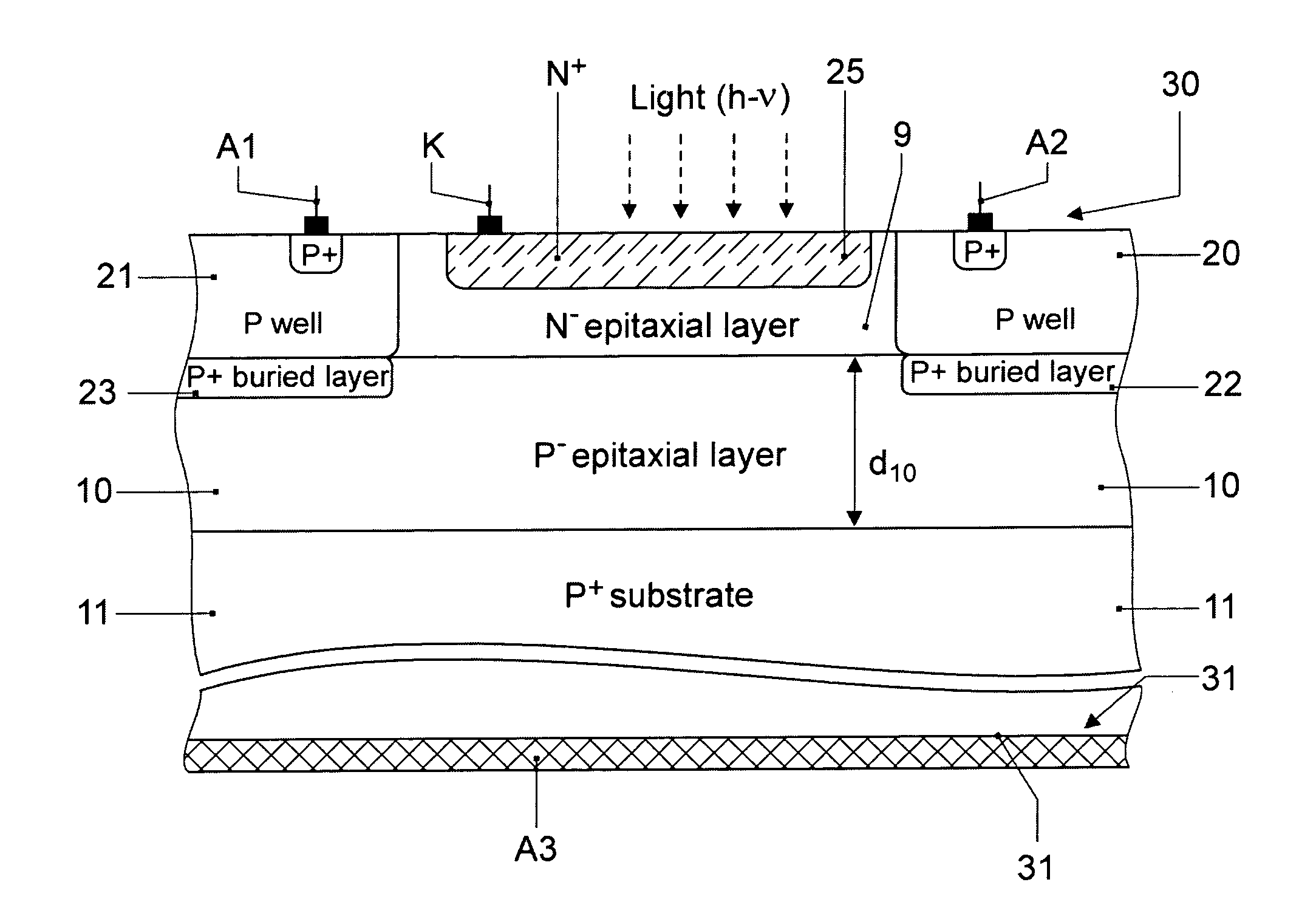
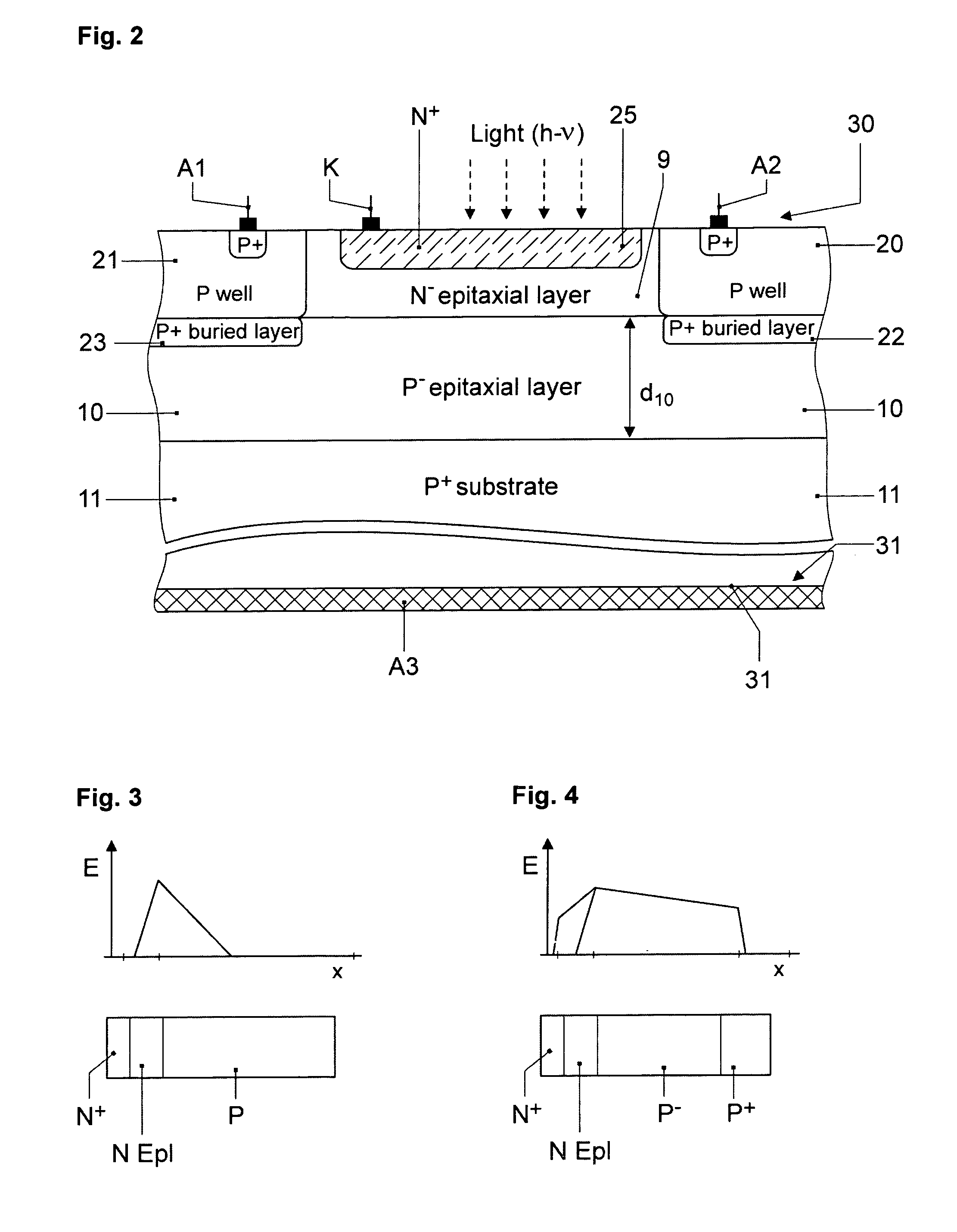
[0021]Existing layers and structures will be discussed in more detail with reference to a further illustrative embodiment according to FIG. 2. FIG. 2 represents a vertical structure of a PIN photodiode. The intrinsic i-zone is formed by two slightly doped epitaxially grown layers 9, 10. The layer following the substrate 11, is a p-type layer. The furthe...


PUM


Abstract

The invention relates to a monolithically integrated vertical pin photodiode which is produced according to BiCMOS technology and comprises a planar surface facing the light and a rear face and anode connections located across p areas on a top face of the photodiode. An i-zone of the pin photodiode is formed by combining a low doped first p-epitaxial layer, which has maximum thickness and doping concentration, placed upon a particularly high doped p substrate, with a low doped second n− epitaxial layer that borders the first layer, and n+ cathode of the pin photodiode being integrated into the second layer. The p areas delimit the second n epitaxial layer in a latent direction while another anode connecting area of the pin diode is provided on the rear face in addition to the anode connection.

Description

FIELD OF THE INVENTION[0001]The present invention relates to an improved vertical PIN photodiode monolithically integrated in a biCMOS technology and to a method of forming the same.BACKGROUND OF THE INVENTION[0002]Discrete PIN photodiodes having a slightly doped i-zone with a thickness of several tens of micrometers formed in silicon technology represent prior art. With PIN photodiodes monolithically integrated into silicon chips, however, the problem to be solved is that the dopant concentration of the substrate ranges from 1015 cm−3 and even higher for CMOS wells and n-collectors / epitaxial layers of npn transistors formed in bipolar and biCMOS technology. For this reason, in non-modified SBC (standard buried collector) technology, processes based on bipolar and biCMOS technology, merely PIN photodiodes are feasible which have a thin i-zone (approximately 1 μm in sophisticated processes), thereby resulting in a low efficiency of approximately 26% at 650 / 670 nm and even less at lon...

Claims


Application Information

Patent Timeline
Patent Type & Authority Patents(United States)
IPC IPC(8): H01L29/868H01L21/8249H01L31/0224H01L31/0352H01L31/105
CPCH01L31/105H01L31/1055
Inventor EINBRODT, WOLFGANGZIMMERMANN, HORSTFOERTSCH, MICHAEL
Owner X FAB SEMICON FOUNDRIES
Learn More