Fine pitch electrical interconnect assembly

a technology of electrical interconnections and assembly parts, applied in the direction of coupling device connections, sustainable manufacturing/processing, final product manufacturing, etc., can solve the problems of increasing difficulty and expense in printing circuit board manufacturing, increasing the concern of impedance mismatch, and reducing pitch. , to achieve the effect of reducing cost and increasing pitch

Active Publication Date: 2009-05-26
R&D SOCKETS INC
View PDF159 Cites 77 Cited by
  • Summary
  • Abstract
  • Description
  • Claims
  • Application Information

AI Technical Summary

Benefits of technology

[0009]In another embodiment, a flexible circuit is interposed between the socket assembly and a printed circuit board. The flexible circuit includes on one side an array of contact pads arranged at a pitch that corresponds with the socket assembly and on the other side an array of contact pads that correspond to a larger pitch on the printed circuit board. This approach permits larger pitch and lower cost printed circuit boards to be used with high performance socket assemblies.
[0013]In one embodiment, the flexible circuit members is compressively retained between the socket assembly and the second circuit member. Additional circuit members are optionally electrically coupled to the flexible circuit member. In another embodiment, the flexible circuit member acts as a sealing layer to substantially prevent solder from wicking along the contact members into the socket assembly. The flexible circuit member preferably includes at least one dielectric layer covering at least a portion of the electrical traces.

Problems solved by technology

This decrease in pitch creates at least two major problems.
First, it is difficult and expense to manufacture printed circuit boards with pitches on the order of about 0.4 mm to about 0.5 mm that correspond to the pitch of high performance socket assemblies.
Second, there are times during the validation and testing of integrated circuits where the user of such socket assemblies may desire to isolate individual signals or a group of signals independently from the routing of the associated printed circuit board (“PCB”).
Test socket contact-resistance (Cres) and impedance mismatch is becoming of greater concern and spring probes have reached their electrical limits.
In many cases, there is no convenient location to place the probe access point on the top surface of the PCB, so designers locate points on the underside of the PCB near the device.
This problem is compounded by the increase in multi-chip packages.

Method used


Image

  • Fine pitch electrical interconnect assembly
  • Fine pitch electrical interconnect assembly
  • Fine pitch electrical interconnect assembly

Examples


Embodiment Construction

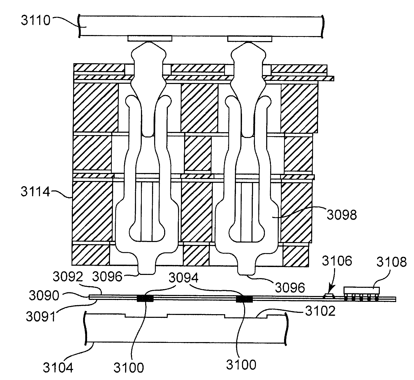
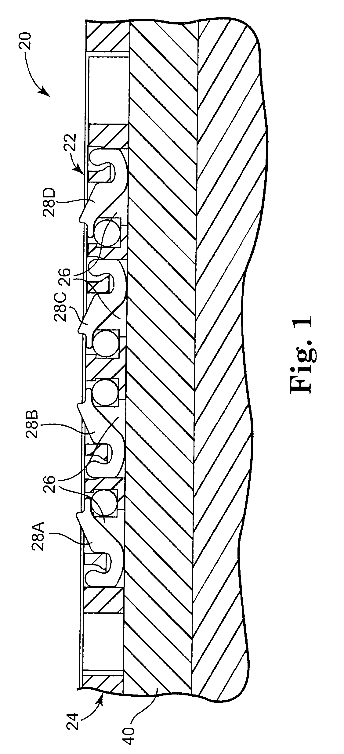
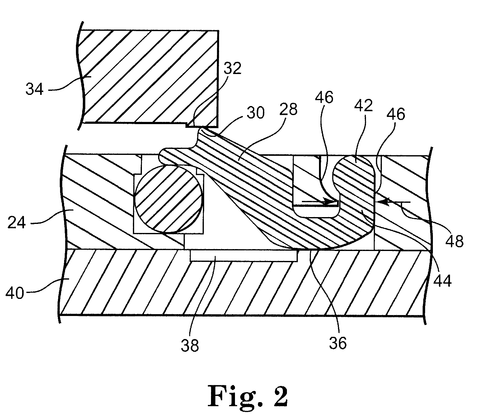
[0092]The present invention is directed to a technique for creating an insulator housing in low, medium, or high volume by laminating layers of precisely patterned materials. The patterned layers can be constructed from the same or multiple material types. The layers are optionally selectively laminated to relieve stress caused by thermal expansion differentials.

[0093]The present construction method permits internal features that would normally be impossible to mold or machine. For large pin count devices, the laminating process produces an inherently flat part without requiring molds. Stiffening layers made of materials such as BeCu, Cu, ceramic, or polymer filled ceramic can be added to provide additional strength and to provide thermal stability during solder reflow.

[0094]The multi-layered housing can also include circuitry layers. Power, grounding and / or decoupling capacitance can be added between layers or between pins, and unique features such as embedded IC devices or RF ante...


PUM


Abstract

An electrical assembly including a socket assembly, a first circuit member electrically coupled to contact members along a first side of a socket assembly, and a second circuit member electrically coupled to the contact members along a second side of the socket assembly. A flexible circuit member is interposed between the socket assembly and the second circuit member. The flexible circuit member comprises a plurality of electrical traces electrically coupled with the contact members on the socket assembly. In one embodiment the flexible circuit member comprises a distal portion extending the electrical traces beyond the socket assembly.

Description

[0001]The present application is a continuation-in-part of U.S. Ser. No. 11 / 935,084 entitled Fine Pitch Electrical Interconnect Assembly filed Nov. 5, 2007, which is a divisional of U.S. Ser. No. 11 / 253,510 entitled Fine Pitch Electrical Interconnect Assembly, filed Oct. 19, 2005 (U.S. Pat. No. 7,297,003), which is a continuation-in-part of U.S. Ser. No. 11 / 030,213 entitled Fine Pitch Electrical Interconnect Assembly, filed Jan. 4, 2005 (U.S. Pat. No. 7,326,064), which is a continuation-in-part of PCT / US2004 / 022886 entitled Electrical Interconnect Assembly with Interlocking Contact System, filed Jul. 15, 2004, which claims the benefit of U.S. Provisional Patent application Ser. No. 60 / 487,630, entitled Snap-in Retention Contact System, filed Jul. 16, 2003, and the present application claims the benefit of U.S. provisional application Ser. No. 60 / 909,550 entitled Logic Analyzer Interface for High Performance Socket, filed Apr. 2, 2007, all of which are hereby incorporated by referenc...

Claims


Application Information

Patent Timeline
Patent Type & Authority Patents(United States)
IPC IPC(8): H01R12/00
CPCH01R13/2414H01R13/2435H05K3/3426H01R9/096H05K2201/10984H05K2203/041H01R12/52Y02P70/50
Inventor RATHBURN, JAMES J.
Owner R&D SOCKETS INC
Why Eureka
Try Eureka