

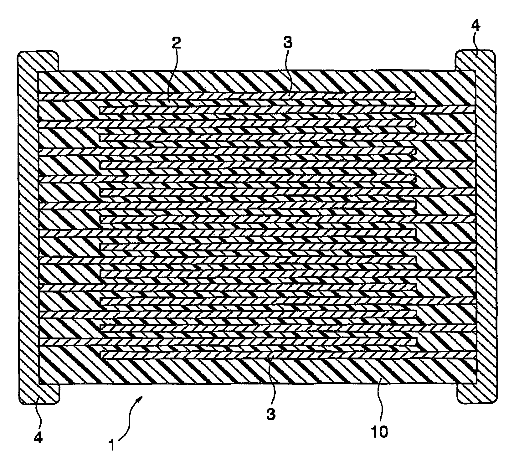
Ceramic electronic device and the production method
a technology of ceramic electronic devices and production methods, applied in the direction of solid-state devices, fixed capacitors, domestic applications, etc., can solve the problems of reducing the insulation resistance (ir), reducing the dielectric layer, and oxidizing the electrodes when fired in the air, and achieve excellent high temperature load lifetime, low ir defect rate, and high reliability
- Summary
- Abstract
- Description
- Claims
- Application Information
AI Technical Summary
Benefits of technology
Problems solved by technology
Method used
Image

Examples
example 1
[0120]As a main component, a dielectric oxide having a composition expressed by {{Ba(1-x)Cax}O}A{Ti(1-y-z)ZryMgz}BO2 was prepared by the sol-gel synthetic method, so that marks “x”, “y”, “z”, “A” and “B” indicating composition ratios become the values below.
[0121]x=0.01
[0122]y=0.18
[0123]z≦0.003
[0124]A / B=1.004
[0125]Next, as a subcomponent, SiO2, MnO, Y2O3, V2O5 and WO3 were subjected to wet grinding by a ball mill for 20 hours, preliminary firing at 900° C. for 4 hours in the air, then, wet grinding by a ball mill for 20 hours for disintegrating to obtain additives of the subcomponent. Note that contents of the respective subcomponent materials in the dielectric layer after firing were adjusted to be the amounts below.
[0126]SiO2: 0.3 wt %
[0127]MnO: 0.2 wt %
[0128]Y2O3: 0.3 wt %
[0129]V2O5: 0.04 wt %
[0130]WO3: 0.05 wt %
[0131]Then, the main component and the adjusted subcomponents were subjected to wet grinding by a ball mill for 19 hours and dried to obtain a dielectric material.
[0132]N...
example 2
[0157]Other than changing an adding amount of SiO2 as a subcomponent to 0.2 wt % and the holding temperature at firing to 1265° C., samples 11 to 18 of the multilayer ceramic capacitor were produced in the same way as in the example 1, and measurement of the IR defect rate, high temperature load lifetime and C.V. value of SiO2 was made in the same way as in the example 1. Note that in the samples 11 to 18 in the present example, the same SiO2 as those in the samples 1 to 8 in the example 1 were used, respectively.
[0158]
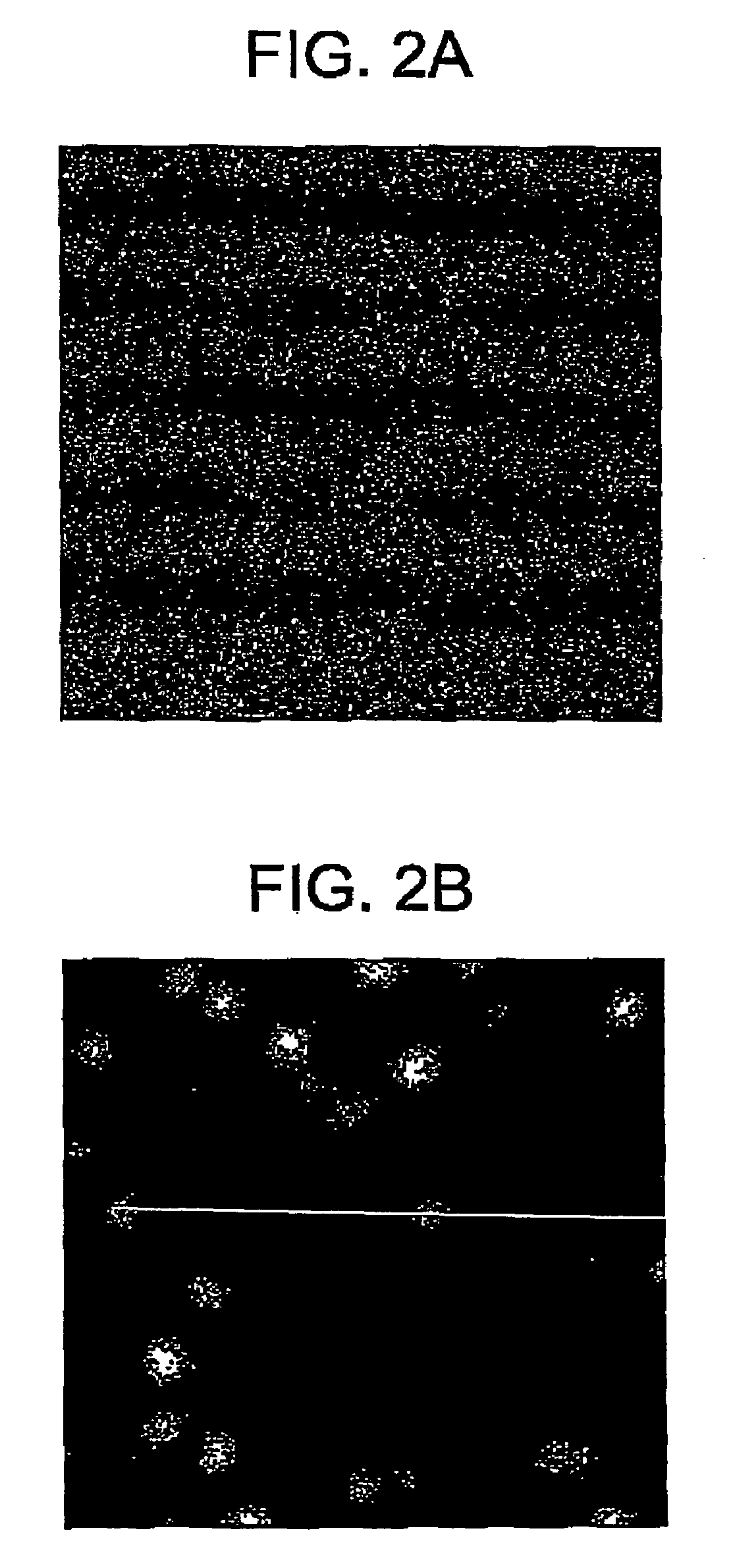
TABLE 2SiO2AddingMaximumFiringAverageCV valueSampleAmountDiameterD100D100 − D50TemperatureIR DefectLifetimeof Si afterNo.[wt %][μm]D50 [μm][μm][μm][° C.]Rate [%][h]Firing [%]11Reference0.22.50.82.51.71265767.2260Example12Example0.22.20.92.21.31265508.722413Example0.21.70.81.70.91265321120614Example0.21.40.71.50.812652112.418915Example0.21.00.31.10.812651018.114516Example0.20.50.41.10.71265026.711917Example0.20.30.31.00.7126503210018Reference0.20.051.06.25.21265803.129...
PUM
| Property | Measurement | Unit |
|---|---|---|
| area | aaaaa | aaaaa |
| area | aaaaa | aaaaa |
| particle diameter | aaaaa | aaaaa |
Abstract
Description
Claims
Application Information