Check patentability & draft patents in minutes with Patsnap Eureka AI!

Image sensor and digital camera

a digital camera and image sensor technology, applied in the field of image sensor and digital camera, can solve the problems of reducing the receiving area of reducing imaging sensitivity, and difficult to focus both visible light and infrared light with excellent characteristics, so as to reduce imaging sensitivity, increase power consumption and/or cost, the effect of deteriorating focusing characteristics

Inactive Publication Date: 2009-05-26
FUJIFILM CORP
View PDF12 Cites 10 Cited by
  • Summary
  • Abstract
  • Description
  • Claims
  • Application Information

AI Technical Summary

Benefits of technology

Enables effective imaging of different wavelengths without reducing sensitivity or increasing power consumption or equipment size, by allowing light to be incident on both faces of the image sensor and using filter layers to manage light paths, thus improving focusing and reducing costs.

Problems solved by technology

Therefore, in comparison with a case of receiving only visible light or only non-visible light at the same light-receiving surface, light-receiving areas for both visible light and infrared light are smaller and imaging sensitivity is lowered, which is a problem.
Consequently, it is difficult to focus both the visible light and the infrared light with excellent characteristics, which is a problem.
As well as leading to increases in power consumption and costs, this leads to an increase in size of the equipment, and these are problems.

Method used


Image

  • Image sensor and digital camera
  • Image sensor and digital camera
  • Image sensor and digital camera

Examples


first embodiment

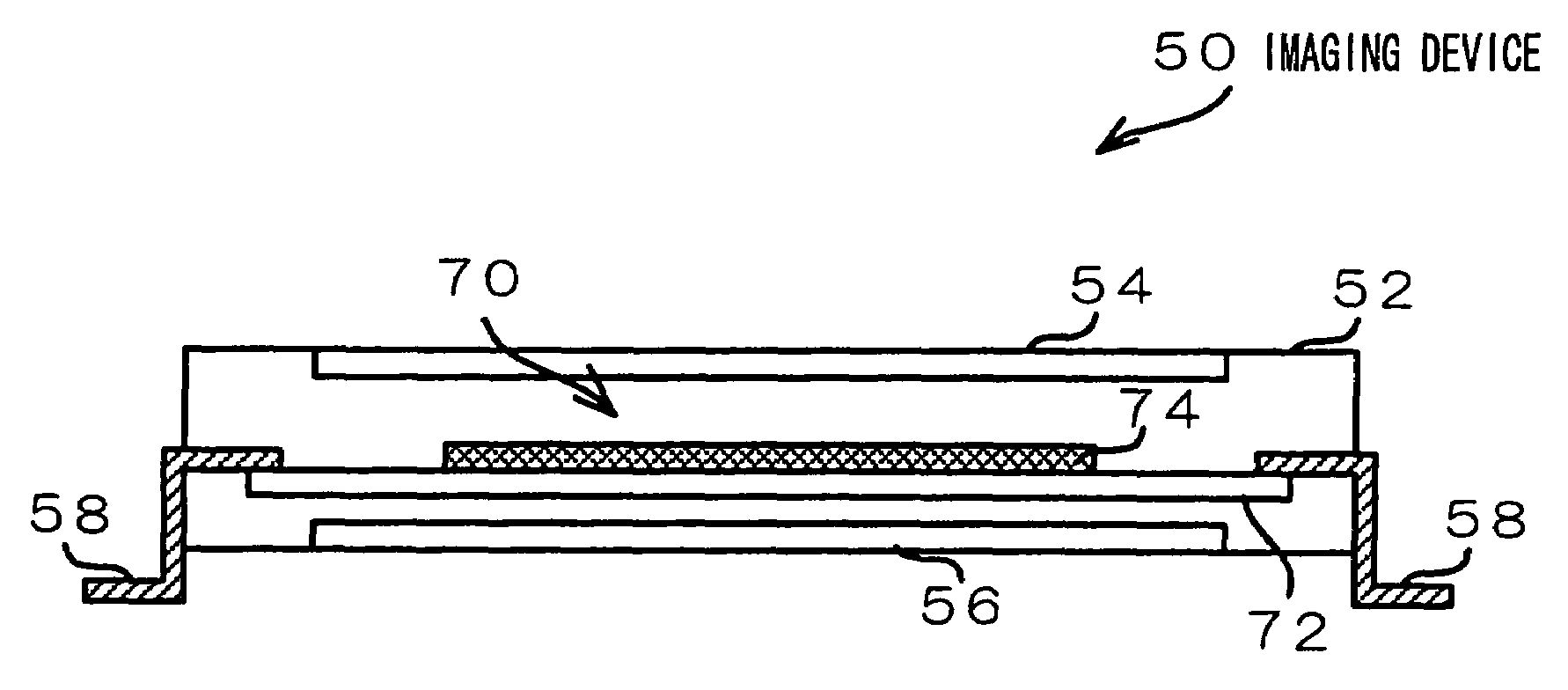
[0027]First, overall structure of an imaging device 50 relating to the present embodiment will be described with reference to the structural side view of FIG. 1.

[0028]As shown in FIG. 1, the imaging device 50 relating to the present embodiment is structured with an image sensor 70 which has been sealed in a case 52. The image sensor 70 is integrally structured by a glass substrate 72 and a sensor portion 74. A transparent glass plate 54 is provided at a front face of the case 52 and a transparent glass plate 56 is provided at a rear face of the case 52.

[0029]The sensor portion 74 is supported at the middle of the imaging device 50, and is provided with plural light-receiving elements in a matrix pattern corresponding to respective pixels. The glass substrate 72 forms electrical connections between the sensor portion 74 and electrodes (terminals) 58 of the imaging device 50, and performs the function of reinforcing the sensor portion 74.

[0030]The sensor portion 74 is capable of recei...

second embodiment

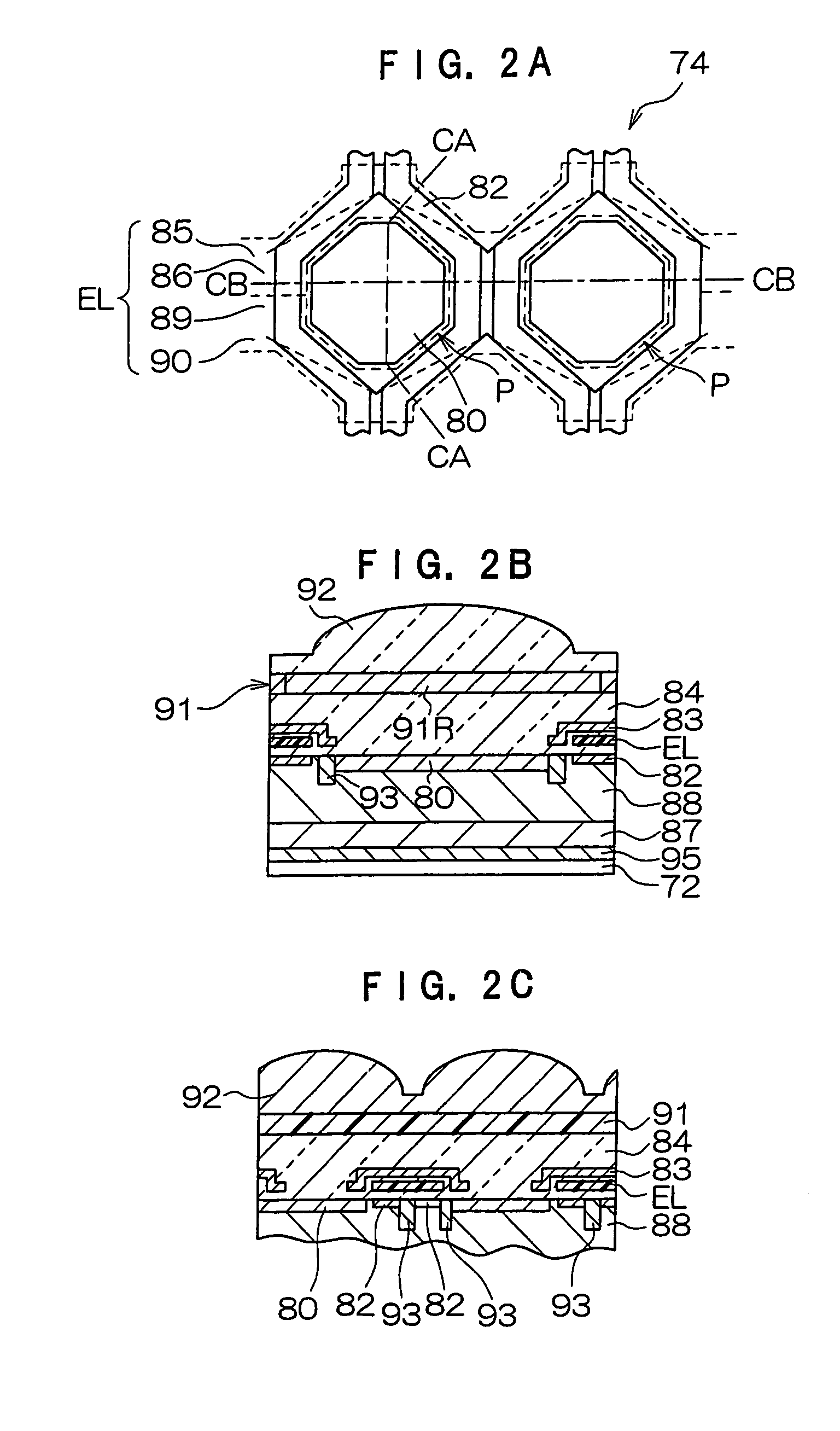
[0075]For this second embodiment, another example of the color filter layer and non-visible light filter layer provided at the image sensor will be described. Structure of the image sensor 70 relating to this second embodiment is the same as the image sensor 70 relating to the first embodiment except in structures of the color filter layer and the non-visible light filter layer. Firstly, structures of a color filter layer 91′ and a non-visible light filter layer 95′ relating to this second embodiment will be described with reference to FIGS. 6A and 6B.

[0076]As shown in FIG. 6A, the color filter layer 91′ relating to the present embodiment is structured by arraying plural sets in a matrix pattern, each set being one each of the red region 91R and the blue region 91B and two of the green region 91G On the other hand, as shown in FIG. 6B, the non-visible light filter layer 95′ relating to the present embodiment is structured by arraying the non-visible light regions 95I in corresponden...


PUM


Abstract

The present invention provides an image sensor that includes a plurality of light-receiving elements and a charge output component. The plurality of light-receiving elements are disposed inside the image sensor in a matrix arrangement corresponding to respective pixels. The light-receiving elements each includes a light-receiving surface at a front face and accumulates charge in accordance with light amounts received at the light-receiving surface. The charge output component outputs the charges accumulated at the plurality of light-receiving elements to outside the image sensor. The image sensor is configured to enable incidence of light on rear faces of the plurality of light-receiving elements. The plurality of light-receiving elements are capable of accumulating charges in accordance with light amounts received at the rear faces.

Description

CROSS-REFERENCE TO RELATED APPLICATION[0001]This application claims priority under 35 USC 119 from Japanese Patent Application No. 2006-248980, the disclosure of which is incorporated by reference herein.BACKGROUND OF THE INVENTION[0002]1. Field of the Invention[0003]The present invention relates to an image sensor and a digital camera, and more particularly to a charge accumulation-type image sensor, which accumulates charges in accordance with light amounts of incident light, and a digital camera which employs this image sensor.[0004]2. Description of the Related Art[0005]In recent years, with increases in resolutions of solid state imaging devices, such as CCD (charge coupled device) area sensors, CMOS (complementary metal oxide semiconductor) image sensors and the like, demand has rapidly increased for information technology devices with photography functions, such as digital electronic still cameras, digital video cameras, portable telephones, PDAs (personal digital assistants,...

Claims


Application Information

Patent Timeline
Patent Type & Authority Patents(United States)
IPC IPC(8): H01L27/00H01L27/14H01L27/148H04N23/12H04N25/00H04N101/00
CPCH01L27/14621H04N5/332H04N9/045H01L27/14618H01L2924/0002H01L27/14647H04N23/11H04N25/134H04N25/133H01L2924/00H04N23/12
Inventor WATANABE, MIKIO
Owner FUJIFILM CORP
Features
  • R&D
  • Intellectual Property
  • Life Sciences
  • Materials
  • Tech Scout
  • Unparalleled Data Quality
  • Higher Quality Content
  • 60% Fewer Hallucinations
Learn More