Planar lenses for integrated optics

a technology of integrated optics and lenses, applied in the direction of lenses, optical elements, instruments, etc., can solve the problems of reducing spatial resolution, affecting the performance of touch screen, and unable to cool down beams, etc., and achieve uniform power distribution

Inactive Publication Date: 2009-06-09
ZETTA RES & DEV LLC RPO SERIES
View PDF18 Cites 20 Cited by
  • Summary
  • Abstract
  • Description
  • Claims
  • Application Information

AI Technical Summary

Benefits of technology

[0012]Advantageously, this aspect of this disclosure enables the guided light passing through the optical element to expand / diverge at a greater angle, thereby providing a more uniform power distribution.
[0019]Advantageously, this aspect is directed to improving the tolerances of an optical element incorporating a planar lens to design and / or assembly errors and variations in ambient temperature.

Problems solved by technology

Referring to FIG. 2, one problem that has been encountered with the prior art design is that the collimated beams may not in fact “fill” curved faces 12 of lens elements 10, but instead form discrete beams 20 separated by considerable dark regions 21.
Whatever the cause, the insufficient divergence causes problems in both the manufacture and performance of the touch screen.
A manufacturing problem arises because when the transmitted light is in the form of discrete beams, the receive-side lens array needs to be critically aligned (in the horizontal plane) with the transmit-side lens array, so that each receive-side lens collects a discrete beam.
The performance problem is one of diminished spatial resolution.
However if the transmitted light is in the form of discrete beams, there are significant “dark” areas from which no blockage can be detected and therefore it is very difficult to interpolate with a grey scale algorithm.
Additionally, the touch sensor cannot detect a touch event in the “dark” areas where there is no light transmitted.
However in the context of optical touch screens this is often undesirable owing to the physical constraints on the width of the transmit and receive arrays (since the waveguides turn through a right angle, lens length translates directly to array width and it is necessary to fit the waveguide array in a screen bezel).
A second problem with the prior art lens design shown in FIG. 1 is that it is a high magnification system, ie. one in which the image distance is much greater than the object distance.

Method used


Image

  • Planar lenses for integrated optics
  • Planar lenses for integrated optics
  • Planar lenses for integrated optics

Examples


example 2

[0072]With reference to FIG. 7a and FIG. 7b, the dimensions of an example composite lens 30 according to the first aspect of the present invention, fabricated via the procedure described in Example 1 and comprising a diverging lens 32 followed by a converging lens 31, will be described. With reference to FIG. 7a, the width 70 of waveguide 33 entering composite lens 30 at point 35 is 8 μm. Converging lens 31 has a flared section 71 of length 300 μm, a straight section 72 of length 1160 μm, a width 73 of 750 μm, and ends in a curved surface 74 that is an arc of a circle with radius of curvature 570 μm. With reference to FIG. 7b, diverging air lens 32 is a bi-convex structure with width 75 of 80 μm and length 76 of 16 μm, is composed of two circular arcs 77 of radius of curvature 100 μm and is positioned a distance 78 of 130 μm from point 35. In the geometrical optics picture, diverging lens 32 forms a virtual image between itself and point 35, and this virtual image serves as the obje...

example 1

COUNTER-EXAMPLE 1

[0074]A low refractive index polymer A and a high refractive index polymer B were prepared as in Example 1. To fabricate a simple transmit lens element 41 of the prior art, as shown in FIG. 4b, polymer A was spin coated onto a silicon wafer and cured with UV light from a mercury lamp, to form a lower cladding layer 20 μm thick and with a refractive index of 1.492 (at 20° C. and 850 nm). Polymer B was spin coated onto the lower cladding to form a core layer 11 μm thick, and patterned with UV light through a mask; the unexposed polymer B material was then dissolved in isopropanol to form waveguide 43 with width 400 of 8 μm and lens element 41 with width 401 of 0.75 mm and length 48 of 2.0 mm. Exposed polymer B material had a refractive index of 1.519 (at 20° C. and 850 nm). Lens element 41 ends in curved surface 45 that is an arc of a circle with radius of curvature 0.655 mm. Refraction at curved surface 45 (a single spherical interface) is governed by the following e...

example 3

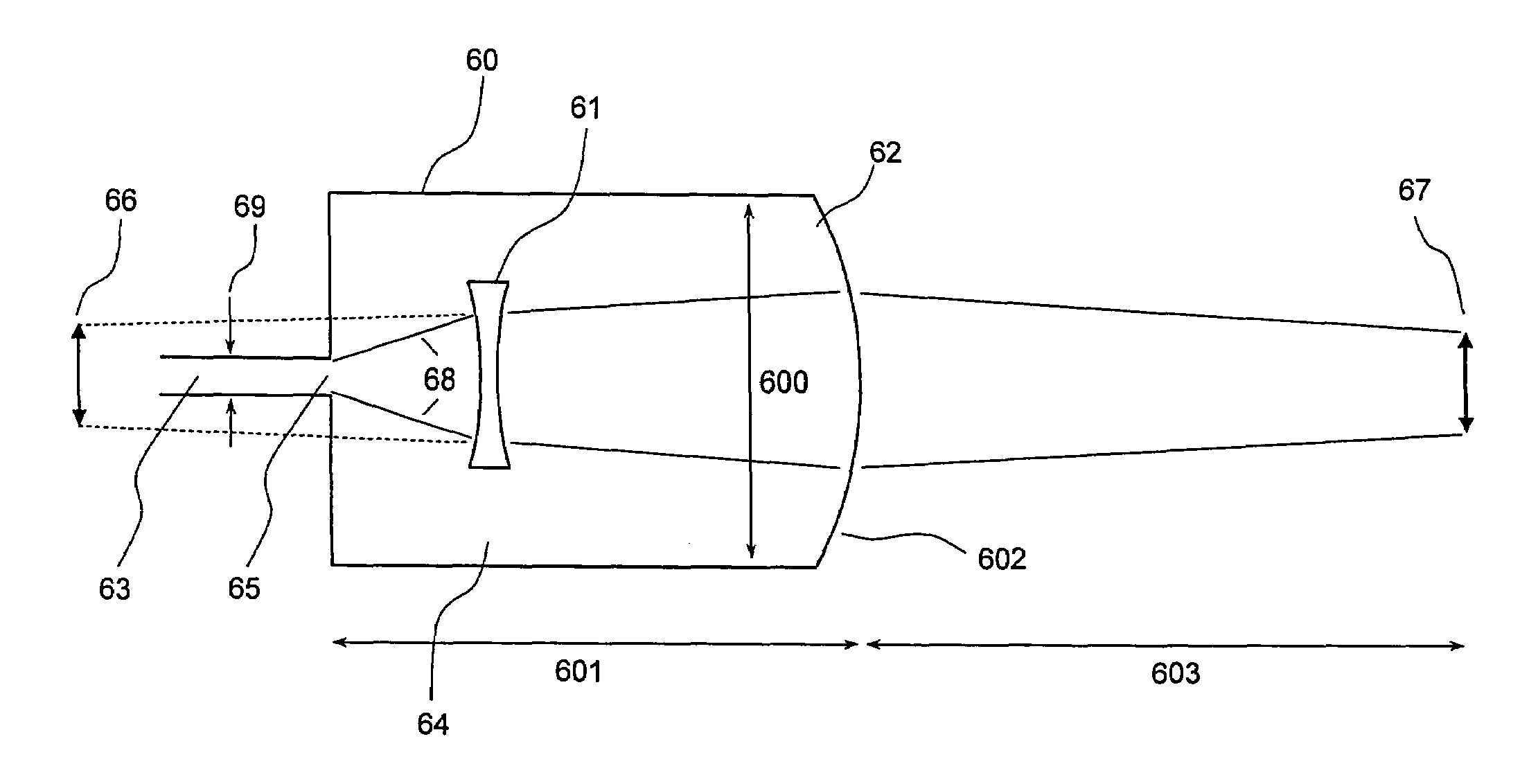
[0082]A low refractive index polymer A and a high refractive index polymer B were prepared as in Example 1. To fabricate a composite transmit lens element 60 according to the second aspect of the present invention, as shown in FIG. 6, polymer A was spin coated onto a silicon wafer and cured with UV light from a mercury lamp, to form a lower cladding layer 20 μm thick and with a refractive index of 1.492 (at 20° C. and 850 nm). Polymer B was spin coated onto the lower cladding to form a core layer 11 μm thick, and patterned with UV light through a mask; the unexposed polymer B material was then dissolved in isopropanol to form a waveguide 63 with width 69 of 8 μm and composite lens element 60 with width 600 of 0.75 mm and length 601 of 2.5 mm. Exposed polymer B material had a refractive index of 1.519 (at 20° C. and 850 nm). Body 64 of composite lens contains a first converging lens 61 composed of air, and ends with curved surface 602 that forms a second converging lens 62. In this E...


PUM


Abstract

Planar lenses for integrated optics applications, in particular for use in optical touch screen sensors are disclosed. The disclosed planar lenses include a slab waveguide and an optical waveguide, preferably formed in unitary fashion, wherein the slab waveguide has a curved end face to focus light into or out of the optical waveguide, and wherein at least one additional lens is included within the slab waveguide. In one aspect of this disclosure, the additional lens is a diverging lens. In a second aspect the additional lens is a converging lens. The additional lens may match the acceptance angle of the optical waveguide to the curved end face of the slab waveguide. Alternatively, it may improve the tolerance of the planar lens to design or assembly errors and / or temperature variations. Preferably, the planar lenses are composed of a photo-patternable polymer, and the additional lenses are composed of air.

Description

TECHNICAL FIELD[0001]A composite lens is disclosed for transmitting a beam of light to or from an integrated optical waveguide. The disclosed lens has particular application in the transmission and reception of light beams across an optical touch screen sensor.BACKGROUND TO THE RELATED ART[0002]Any discussion of the related art throughout the specification should in no way be considered as an admission that such prior art is widely known or forms part of common general knowledge in the field.[0003]U.S. Pat. Nos. 5,914,709, 6,181,842 and 6,351,260 describe an optical touch screen sensor in which integrated optical waveguides are used to launch an array of light beams across a screen, then collect them at the other side of the screen and conduct them to a position-sensitive detector. In the design for the “transmit side”, an array of waveguides feeds into a row of lens elements that expand the guided light beams in the horizontal plane, then collimate them in the horizontal plane as t...

Claims


Application Information

Patent Timeline
Patent Type & Authority Patents(United States)
IPC IPC(8): G02B6/32G02B6/10G02B6/26
CPCG02B6/12004G02B6/1221G02B6/124G02B6/1245G02B6/138G02B6/32G06F3/0421G02B2006/12102G02B3/02
Inventor KUKULJ, DAXCORNISH, BENJAMINCHARTERS, ROBERT BRUCEATKINS, GRAHAM ROYLUTHER-DAVIES, BARRY
Owner ZETTA RES & DEV LLC RPO SERIES
Why Eureka
Try Eureka