Low power array multiplier

a low-power array and multiplier technology, applied in the field of array multipliers, can solve the problems of low power consumption, and achieve the effects of reducing power consumption, reducing latency, and reducing power consumption

Inactive Publication Date: 2009-06-09
QUALCOMM INC
View PDF7 Cites 41 Cited by
  • Summary
  • Abstract
  • Description
  • Claims
  • Application Information

AI Technical Summary

Benefits of technology

[0006]The present invention relates to an array multiplier with reduced latency and lower power consumption than conventional array multipliers. The array multiplier comprises a partial product array including a plurality of array elements arranged in rows and columns to compute and aggregate partial sums, and a carry propagate adder including a plurality of adder elements to generate the final result bits. For an N×M bit accurate multiplication, where N and M are the bit widths of the multiplicand and the multiplier respectively, the partial product array comprises N rows and M columns. However there are occasions where data with bit precisions lower than N or M needs to be processed by the same N×M bit multiplier. In such cases, the multiplicand and / or multiplier may be shifted so that not all of the array elements in the partial product array are used. The unused array elements are either turned off or prevented from switching resulting in lower power consumption.
[0007]In some embodiments, additional latency and power savings may be obtained by the addition of bypass lines in the partial product array to bypass unused array elements and / or adder elements that fall in the critical delay path. The internal bypass lines allow internal array elements to directly output result bits without the need of trickling the result bits down through unused array elements and / or adder elements in the critical delay path. In some embodiments, operands may be arbitrarily shifted any amount, i.e., shifted with 1-bit granularity. In these embodiments, the amount that an operand is shifted is dictated by the length of the operand. Maximum savings in latency and power are achieved when the MSB (most significant bit) of the operand is aligned with the most significant row or column of the partial product array. In other embodiments using fewer bypass lines, the amount that an operand is shifted depends on the location of the bypass granularity. In these embodiments, operands may be shifted to align a least significant bit of the operand with a pre-determined row or column of the array. In any event, as long as the bit-precision of an operand is less than the maximum size of the array, a reduction in both power and latency is achieved by the disclosed techniques. Further reduction of power and latency requirements can be achieved if bypass lines are extended beyond the carry propagate adder.

Problems solved by technology

The unused array elements are either turned off or prevented from switching resulting in lower power consumption.

Method used


Image

  • Low power array multiplier
  • Low power array multiplier
  • Low power array multiplier

Examples


first embodiment

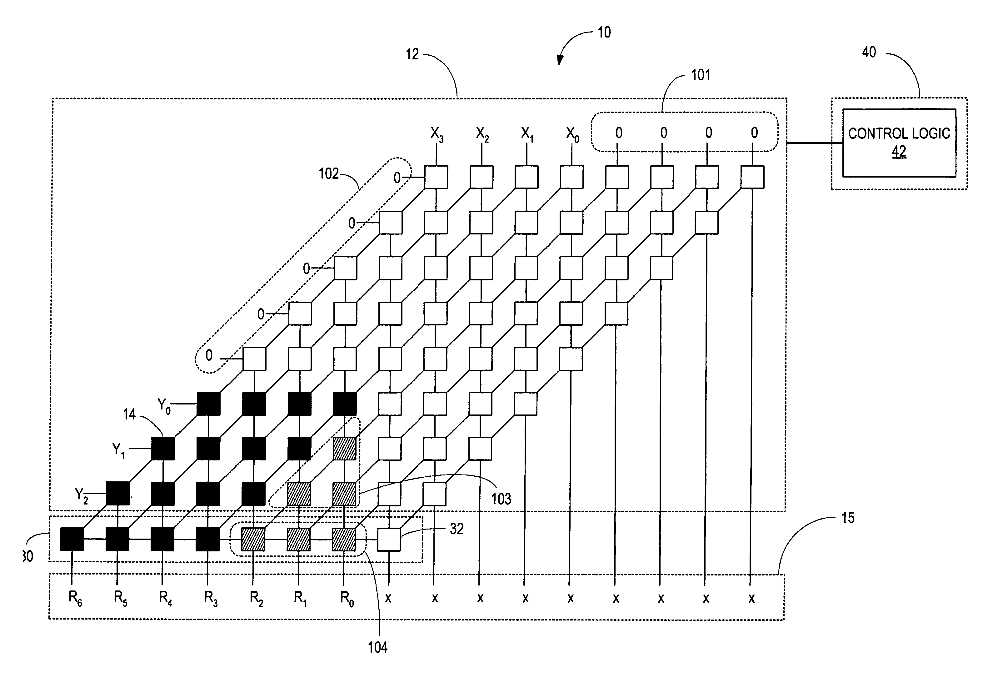
[0037]FIG. 4 illustrates one exemplary method for reducing power dissipated by the array multiplier 10 when the length of one or both operands is less than the maximum length of the partial product array 12. FIG. 4 illustrates multiplication of a 4-bit multiplicand by a 3-bit multiplier using an 8×8 array multiplier 10. As shown in FIG. 4, both the multiplicand and multiplier are input to the partial product array 12 in a shifted position. That is, the operands are shifted towards the most significant column or row of the partial product array 12. In the embodiment shown in FIG. 4, the operands are shifted to align the most significant bit of the operands with the most significant column and row respectively of the partial product array 12. Shifting the operands towards the most significant bit position of the partial product array 12 reduces the number of array elements 14 needed to compute the product of the operands. The array elements 14 and adder elements 32 needed for the comp...

second embodiment

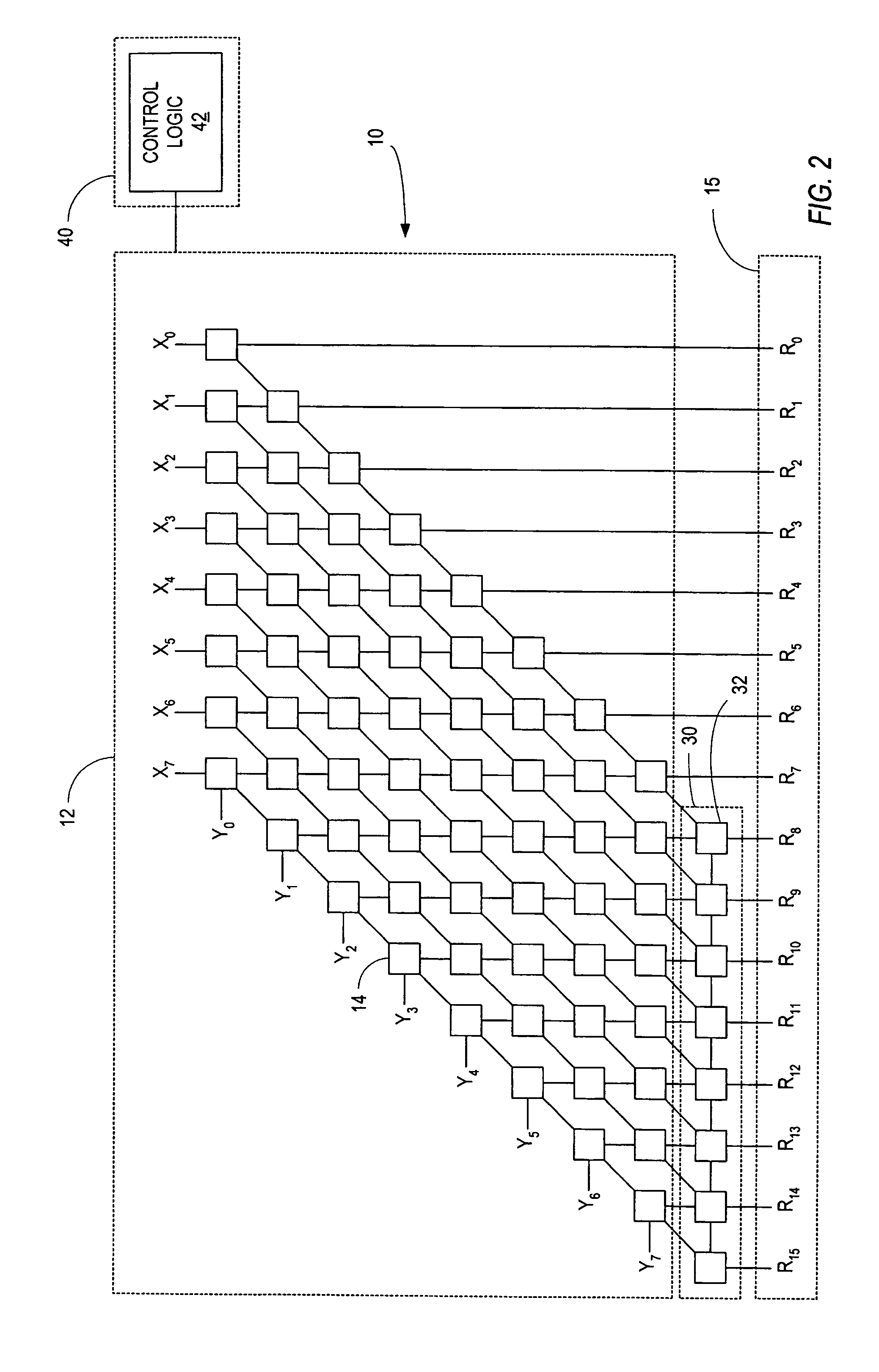
[0042]FIGS. 5-7 illustrate a second exemplary embodiment of the array multiplier 10. The second embodiment is similar to the first embodiment shown in FIGS. 2-4. Therefore, for the sake of brevity and clarity, the same reference numerals will be used to designate similar components in the two embodiments and the discussion below will focus on aspects where the second embodiment differs from the first.

[0043]The array multiplier 10 according to the second embodiment comprises a partial product array 12 including a plurality of array elements 14 arranged in columns and rows, a carry propagate adder 30 including a linear array of adder elements 32, and a control circuit 40. The array elements 14 in the partial product array 12 and the adder elements 32 in the carry propagate adder 30 are interconnected as previously described with the following differences. In the second embodiment of the array multiplier 10, the partial product array 12 includes bypass lines 22 connecting array element...

third embodiment

[0048]The array multiplier 10 shown in FIGS. 5-7 allows operands to be shifted with one-bit granularity. The one-bit granularity allows operands of any size to be shifted completely to align the most significant bits of the operands with the most significant column and row respectively of the partial product array. The bypass lines 22, however, may introduce parasitic capacitance into the partial product array 12. Therefore, it may not be desirable to reduce the number and length of the bypass lines 22.

[0049]FIG. 8 illustrates another embodiment of the array multiplier 10 that uses fewer bypass lines 22 and thus reduces parasitic capacitance, but which has a coarser granularity. Array multiplier 10 comprises a partial product array 12 including a plurality of array elements 14, a carry propagate adder 30 including a linear array of adder elements 32, and a control circuit 40 as previously described. The control circuit 40 includes control logic 42 and control register 44 that operat...


PUM


Abstract

An array multiplier comprises a partial product array including a plurality of array elements and a final carry propagate adder. Operands smaller than a corresponding dimension of the partial product array are shifted toward the most significant row or column of the array to reduce the number of array elements used to compute the product of the operands. Switching activity in the unused array elements may be reduced by turning off power to the array elements or by padding the shifted operands with zeros in the least significant bits. Additional power saving may be achieved by having bypass lines in the partial product array that bypasses non-essential array elements and by feeding partial sum and carry directly to the final carry propagate adder. Elements of the carry propagate adder may also be bypassed to achieve further power reduction.

Description

BACKGROUND OF THE INVENTION[0001]1. Field of the Invention[0002]The present invention relates generally to arithmetic circuits for digital signal processors and more particularly to an array multiplier for computing the product of two operands.[0003]2. Relevant Background[0004]Portable electronic devices have become ubiquitous to modem life. Two relentless trends in portable electronic devices are increased functionality and decreased size. Increased functionality demands require increased computing capability—in particular, ever faster and more powerful processors. Decreased size requires decreasing the size of batteries used to power the processor and other electronics in the device. Therefore, manufacturers are faced with the seemingly contradictory goals of increasing computing capability, and hence power requirements, while at the same time decreasing battery size. While improvements in battery technology partially offset the problem, the decreasing size of batteries and demand...

Claims


Application Information

Patent Timeline
Patent Type & Authority Patents(United States)
IPC IPC(8): G06F7/53
CPCG06F7/5312G06F2207/382G06F2207/3868G06F7/52G06F7/53
Inventor ISLAM, FARHAD FUAD
Owner QUALCOMM INC
Why Eureka
Try Eureka