Light emitting diode package having multi-stepped reflecting surface structure and fabrication method thereof

a technology of light-emitting diodes and reflective surfaces, which is applied in the direction of basic electric elements, electrical equipment, semiconductor devices, etc., can solve the problems of increasing assembly costs and reducing the simplification of the manufacturing process, and achieve the effect of reducing manufacturing costs and simplifying the manufacturing process

Active Publication Date: 2009-06-16
SAMSUNG ELECTRONICS CO LTD
View PDF2 Cites 32 Cited by
  • Summary
  • Abstract
  • Description
  • Claims
  • Application Information

AI Technical Summary

Benefits of technology

[0011]The present invention has been made to solve the foregoing problems of the prior art and therefore an aspect of the present invention is to provide an LED package which has a multi-stepped reflecting surface formed integrally in a substrate to simplify the manufacturing process and reduce the manufacturing costs, and a fabrication method thereof.
[0012]Another aspect of the invention is to provide an LED package which has a multi-stepped reflecting surface structure to achieve superior heat radiation effect through a substrate, allowing application to low power and high power LED chips, thereby significantly increasing the lifetime and light emission efficiency, and a fabrication method thereof.
[0013]According to an aspect of the invention, the invention provides a light emitting diode package which includes: an Al substrate having a recessed multi-stepped reflecting surface formed in a side thereof; a light source comprising light emitting diodes mounted on the reflecting surface and electrically connected to patterned electrodes; anodized insulation layers formed between the patterned electrodes and the substrate; an encapsulant covering over the light source of the substrate; and an Al heat radiator formed under the light emitting diodes of the light source to improve heat radiation capacity.

Problems solved by technology

Furthermore, the conventional LED package 300 has the reflecting member 320 fixed by a separate process to the substrate 310, hindering simplification of the manufacturing process with increased assembly costs.

Method used


Image

  • Light emitting diode package having multi-stepped reflecting surface structure and fabrication method thereof
  • Light emitting diode package having multi-stepped reflecting surface structure and fabrication method thereof
  • Light emitting diode package having multi-stepped reflecting surface structure and fabrication method thereof

Examples


Embodiment Construction

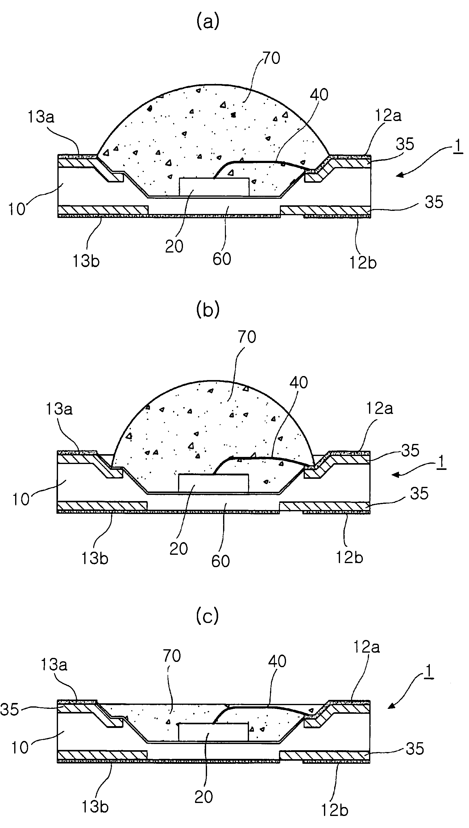
[0033]Exemplary embodiments of the present invention will now be described in detail with reference to the accompanying drawings.

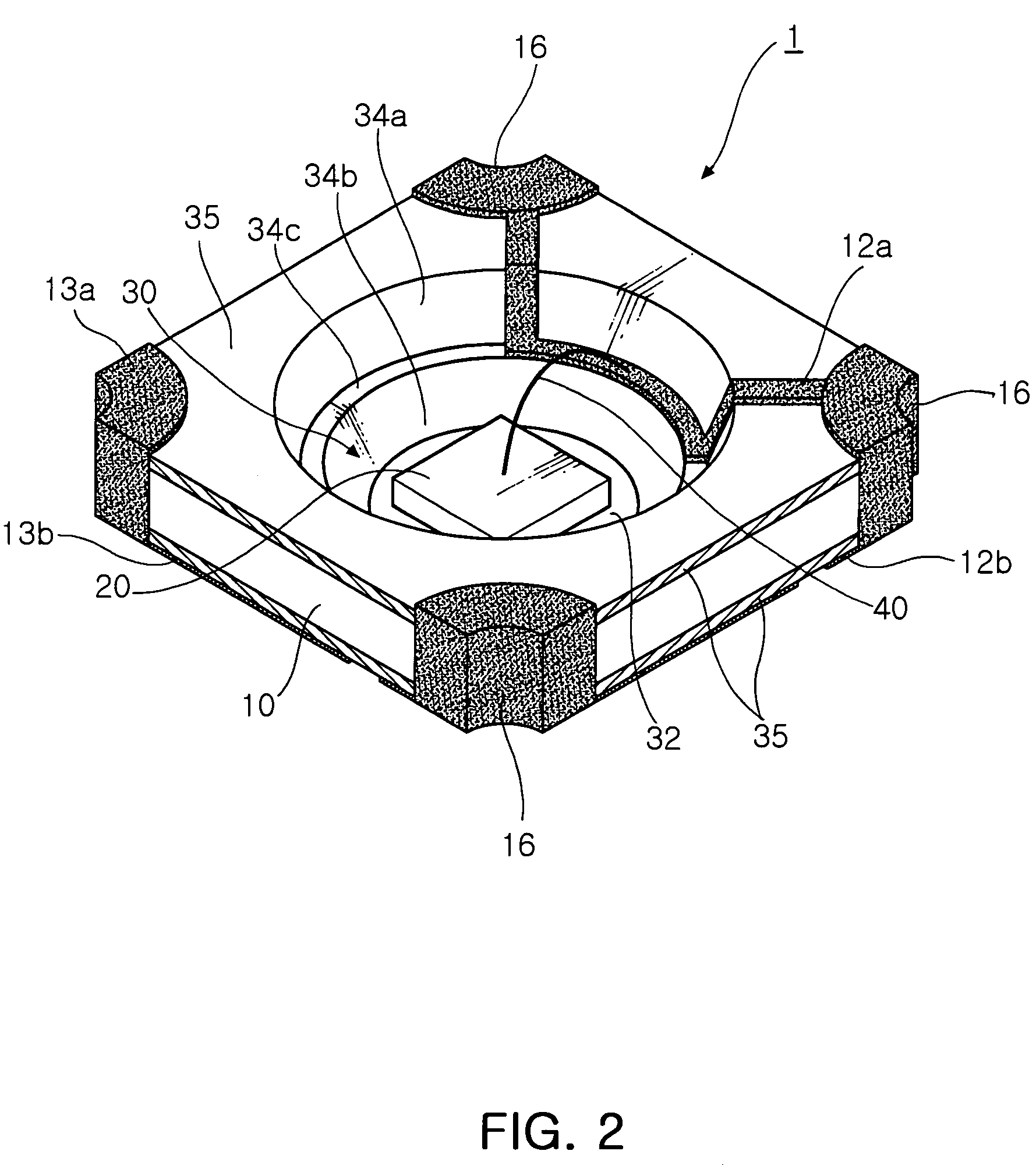
[0034]An LED package 1 having a multi-stepped reflecting surface structure according to the present invention includes a substrate 10 made of an Al material, as shown in FIG. 2. The substrate 10 is made of an Al material which is relatively low-cost and easily manufactured.

[0035]Such a substrate 10 has a reflecting surface 30 formed in a center thereof. The reflecting surface 30 is defined by a recess formed by etching the substrate 10, and includes a planar central reflecting surface portion 32, on which the light source 20 described later is seated, i.e., a die bonding reflecting surface portion and inclined reflecting surface portions 34a and 34b, surrounding the central reflecting surface portion 32, formed in multiple steps.

[0036]In addition, an Ag material, which is highly reflective, is coated on the inclined reflecting surface portions 34a and 34b ...


PUM


Abstract

A high luminance and high output LED package using an LED as a light source and a fabrication method thereof. The LED package includes an Al substrate with a recessed multi-stepped reflecting surface formed therein and a light source composed of LEDs mounted on the reflecting surface and electrically connected to patterned electrodes. The LED package also includes anodized insulation layers formed between the patterned electrodes and the substrate, and an encapsulant covering over the light source of the substrate. The LED package further includes an Al heat radiator formed under the LEDs to enhance heat radiation capacity. According to the present invention, the substrate is made of Al material and anodized to form insulation layers thereon, allowing superior heat radiation effect of the LED, thereby significantly increasing the lifetime and light emission efficiency of the LED package.

Description

CLAIM OF PRIORITY[0001]This application claims the benefit of Korean Patent Application No. 2006-0036099 filed on Apr. 21, 2006, in the Korean Intellectual Property Office, the disclosure of which is incorporated herein by reference.BACKGROUND OF THE INVENTION[0002]1. Field of the Invention[0003]The present invention relates to a high luminance and high output Light Emitting Diode (LED) package using an LED as a light source. More particularly, the invention relates to an LED package having a multi-stepped reflecting surface structure, in which a light source is mounted on an aluminum (Al) substrate and a multi-stepped reflecting surface is integrally formed around the light source to improve the light efficiency and heat radiation effect of an LED during light emitting operation, thereby prolonging the lifetime of the LED while maintaining high luminance and high output of the LED package, and a fabrication method thereof.[0004]2. Description of the Related Art[0005]As shown in FIG...

Claims


Application Information

Patent Timeline
Patent Type & Authority Patents(United States)
IPC IPC(8): H01L29/207H01L33/54H01L33/56H01L33/44H01L33/62H01L33/64
CPCH01L33/483H01L33/60H01L33/641H01L2224/48091H01L2924/00014
Inventor SHIN, SANG HYUNCHOI, SEOG MOONLEE, YOUNG KI
Owner SAMSUNG ELECTRONICS CO LTD
Why Eureka
Try Eureka