
Active matrix structure for display screen and screen comprising one such matrix

Active Publication Date: 2009-06-16
INTERDIGITAL CE PATENT HLDG
View PDF4 Cites 2 Cited by
  • Summary
  • Abstract
  • Description
  • Claims
  • Application Information

AI Technical Summary

Benefits of technology

[0014]An object of the invention is to propose a novel matrix structure of display screens which makes it possible to satisfy the image quality criteria despite a reduced size of the pixel elements without adding constraints of external connection and while retaining good optical quality, in particular a high aperture ratio for each pixel.
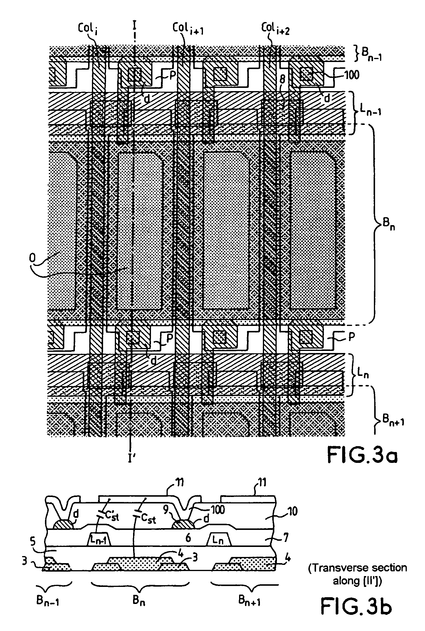
[0022]The connection of the storage bus of a row to a previous selection line makes it possible to maintain the charge on the storage capacitor associated with each pixel electrode at a stable reference value, thereby making it possible to ensure the charging of the pixel electrode of the row to the proper video voltage.
[0025]Through this second gate which follows the voltage level of the selection line of the previous row, the turning off of the transistors to the current row is improved: the leakage currents are in particular limited for the whole duration of the frame time which follows the selection of the current row, when the voltage levels have been charged on the pixel electrodes and the associated storage capacitors, thereby helping to improve the maintaining of the charge on the pixel electrodes, and hence, the quality of the image.
[0026]According to another aspect of the invention, an additional advantage of gate precharging may also be obtained from this double gate transistor structure according to the invention, by ensuring judicious logic for connecting the storage capacitor buses with the row selection lines, as a function of the mode of addressing of the screen: frame inversion, line inversion, double line.
[0027]Thus, with a matrix structure according to the invention comprising a storage capacitor bus under each row of pixel electrodes according to the invention, the matrix fabrication yield, the storage capacitance, and also the driving of the pixels are improved. The optical quality of the screens which use such matrices is thereby improved.
[0028]Preferably, the connection of these buses to the associated row selection line is effected outside the active matrix, at at least one end. The connection of the previous line to the two ends of the bus affords the additional advantage of allowing the self-repair of the row selection lines should they be open, due to a fabrication defect. To improve the transmission of the signal, provision may also be made to connect the storage bus to the previous row selection line, at the level of each pixel electrode. One then compensates for the effects of the high access resistance of the storage buses, that is due to the material used, in the case of a line break.

Problems solved by technology

However, with such storage capacitor structures, the metal of the selection line, which metal is opaque, encroaches onto the surface of the pixel electrode.
This solution turns out to be poorly suited for so-called high resolution screens, for which the pixel elements are already of small dimensions.
Specifically, problems of crossover with the other external signals arise, in particular the scanning signals, thereby rendering the design of the installation scheme more complex.
The pixel electrodes concerned are then short-circuited to the potential of the back electrode: these pixels therefore appear white (or else red, green or blue, in the case of a color screen) These visible defects affect the fabrication yield.

Method used


Image

  • Active matrix structure for display screen and screen comprising one such matrix
  • Active matrix structure for display screen and screen comprising one such matrix
  • Active matrix structure for display screen and screen comprising one such matrix

Examples


Embodiment Construction

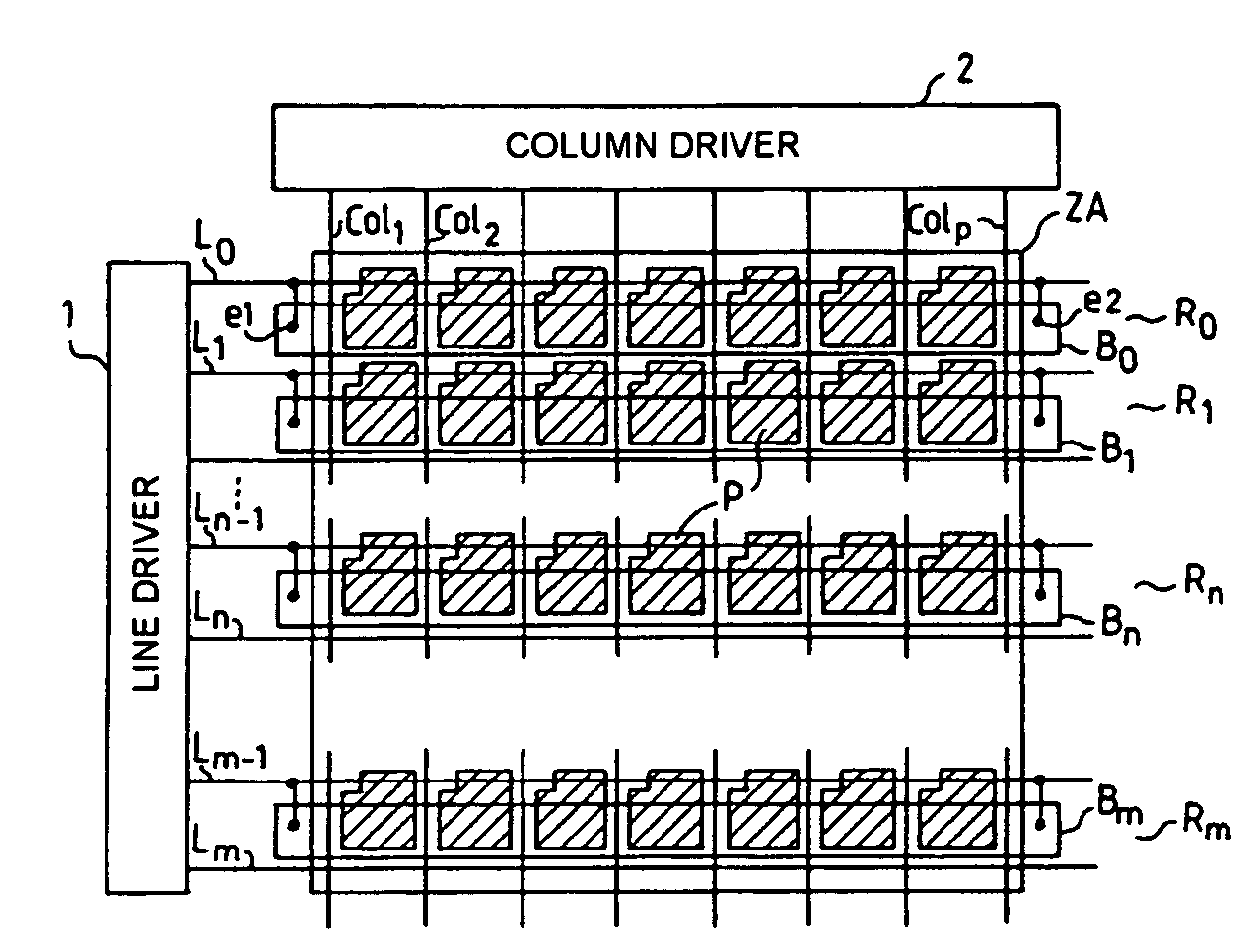
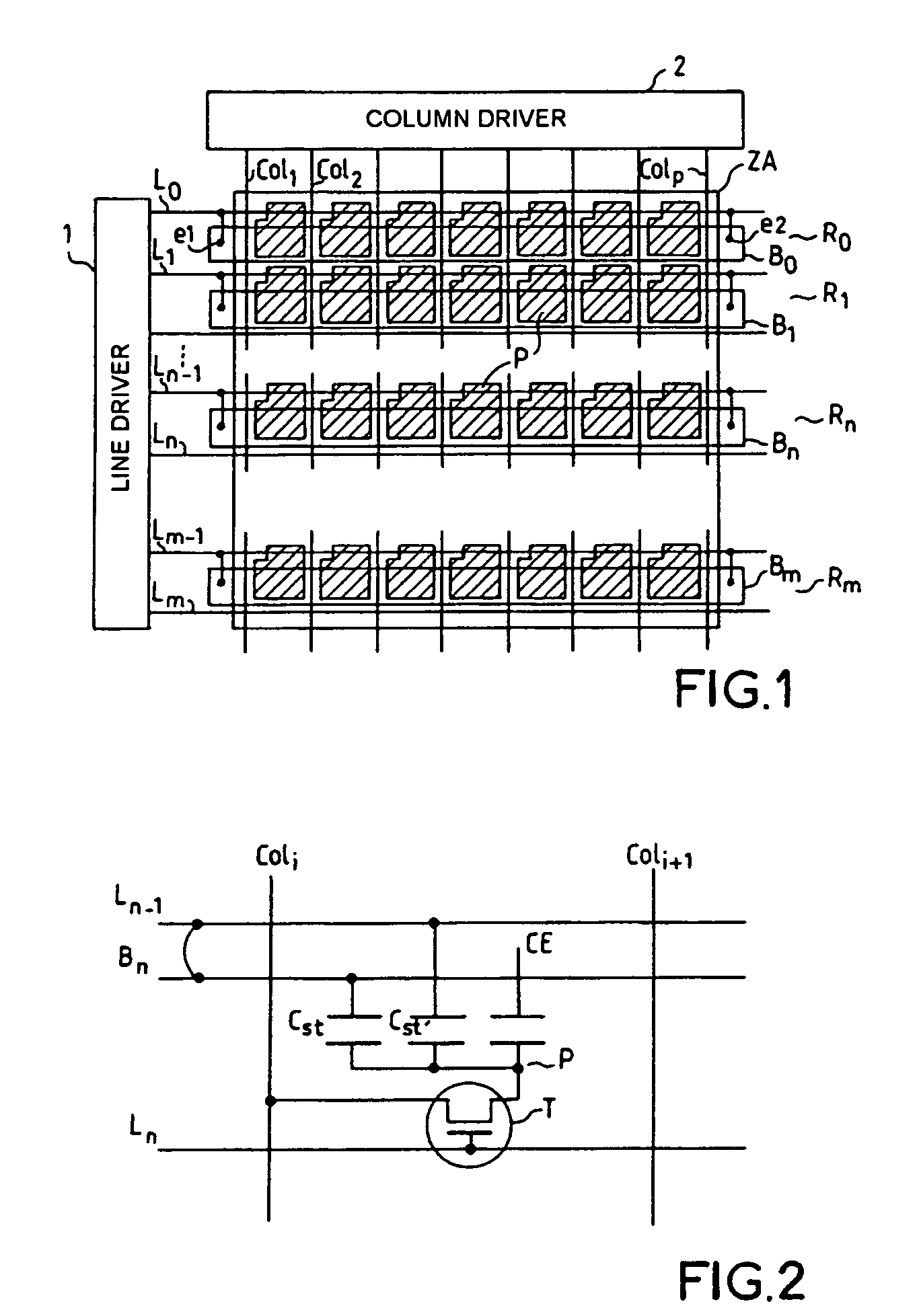
[0042]FIG. 1 diagrammatically represents an active matrix for display screen. Pixel electrodes P are disposed in matrix fashion according to a crossed array of rows L1, . . . Lm, and columns Col1, . . . Colp.

[0043]The rows are selected successively, and the corresponding display data transmitted to the pixel electrodes, by means of drive devices (drivers) 1, 2, well known to the person skilled in the art.

[0044]Each pixel electrode covers a large part of the surface framed by two successive rows and columns. In the figure, row Rn is framed by the associated selection line Ln, and by the selection line Ln−1 of the immediately preceding row.

[0045]According to the invention, for each pixel electrode row, an associated storage capacitor bus Bn is provided under the pixel electrode row, substantially of the same width.

[0046]This bus Bn is therefore disposed in parallel, between two selection lines Ln and Ln−1. It is connected to the selection line Ln−1 of the previous row. In the example ...


PUM


Abstract

An active matrix structure for display screen includes a storage capacitor bus disposed under each row of pixel electrodes, produced in a transparent conducting material, and disposed in the structure on a level separated from a level of the row selection lines and a level of the pixel electrodes by an insulation layer at least. The storage bus of a row is driven by a selection line of a previous row.

Description

BACKGROUND OF THE INVENTION[0001]1. Field of the Invention[0002]The present invention pertains to matrix display screens, and more particularly to an active matrix structure of pixel elements offering both large storage capacity on each pixel electrode and a high aperture ratio. The field of the invention is that of active matrices formed on a transparent substrate.[0003]2. Discussion of the Background[0004]A matrix display screen is customarily formed of two transparent substrates, for example made of glass, facing one another, joined together by a peripheral seal so as to allow a cavity in which is located the display material such as liquid crystals or light-emitting diodes made of organic material (OLEDs as they are known). The first substrate is clad with a back electrode, common to the whole matrix, linked to a reference potential. In the case of a color screen, this substrate furthermore comprises a matrix of colored filters (typically, red, green and blue filters). The secon...

Claims


Application Information

Patent Timeline
IPC IPC(8): G02F1/1343G02F1/1362
CPCG02F1/136213
Inventor KRETZ, THIERRYLEBRUN, HUGUES
Owner INTERDIGITAL CE PATENT HLDG
Learn More