Amplifying-type solid-state imaging device

Inactive Publication Date: 2008-08-07
SHARP KK
View PDF6 Cites 8 Cited by
  • Summary
  • Abstract
  • Description
  • Claims
  • Application Information

AI Technical Summary

Benefits of technology

[0021]Accordingly, an object of the present invention is to provide an amplification type solid-state image pickup device capable of obtaining a low-noise, high-quality image while reducing the number of transistors per pixel to reduce the pixel size.

Problems solved by technology

However, providing three to four MOS transistors per pixel would be a limitation to a reduction of the pixel size.
However, the technique of JP 2005-217607 A is subject to occurrence of the following problem.
However, doing so would lower the gain A in turn, leading to a problem that the charge-voltage conversion efficiency η would decrease.

Method used


Image

  • Amplifying-type solid-state imaging device
  • Amplifying-type solid-state imaging device
  • Amplifying-type solid-state imaging device

Examples


first embodiment

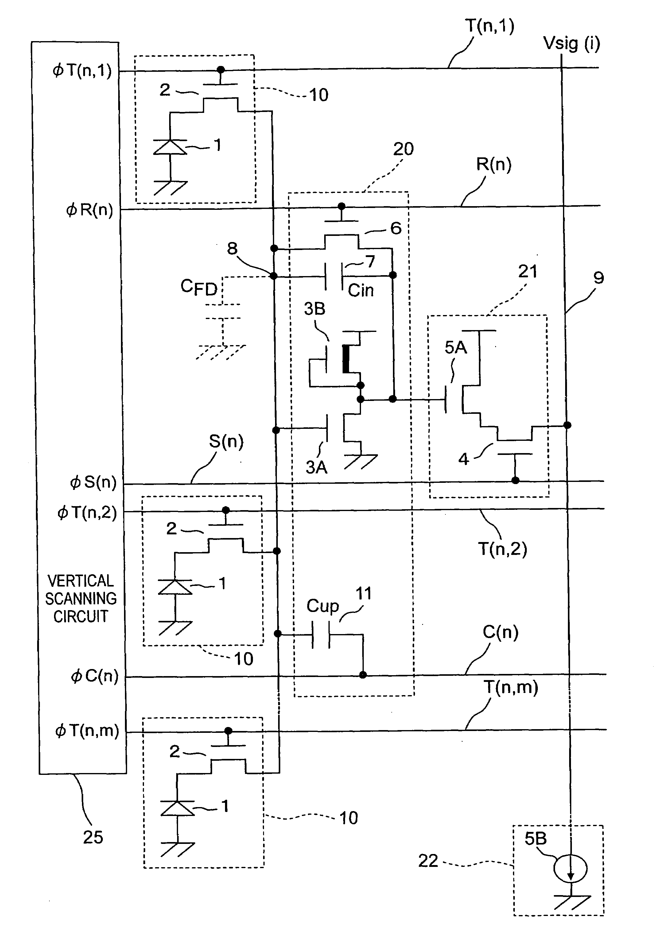
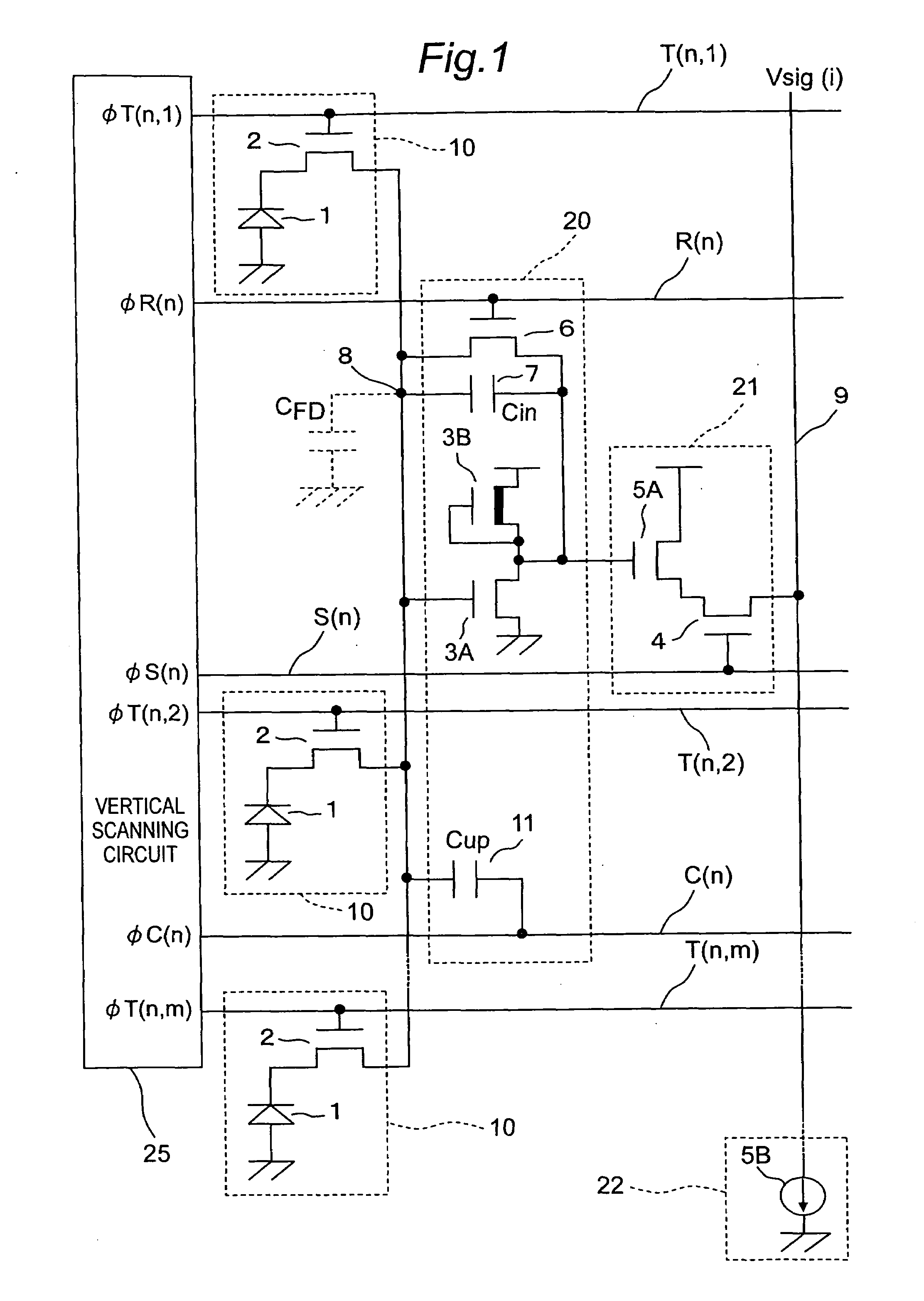
[0075]FIG. 1 is a circuit diagram showing part of a two-dimensional amplification type solid-state image pickup device according to a first embodiment of the invention. Pixels of the device are two-dimensionally arrayed in a matrix, and here is shown an n-th row within an i-th column for simplicity's sake, where m pixels are included in each one row (where m≧2, n≧2 and i≧2).

[0076]FIG. 1 shows a photoelectric conversion section group composed of m photoelectric conversion sections 10 of the i-th column out of a plurality of rows and columns of photoelectric conversion sections 10, one switched capacitor amplifier section 20 connected to the photoelectric conversion section group, and one current amplification section 21 connected to the one switched capacitor amplifier section 20.

[0077]This two-dimensional amplification type solid-state image pickup device, as shown in FIG. 1, is composed of the photoelectric conversion sections 10, the switched capacitor amplifier section 20, the cu...

second embodiment

[0123]FIGS. 5A and 5B are circuit diagrams showing part of a two-dimensional amplification type solid-state image pickup device according to a second embodiment of the invention.

[0124]In the first embodiment, the switched capacitor amplifier section 20 and the current amplification section 21 included in the two-dimensional amplification type solid-state image pickup device are equal in number. However, in this second embodiment, a plurality of select-type switched capacitor amplifier sections 20A share one current amplification section 21. Like component members other than the above in conjunction with the first embodiment are designated by like reference numerals, and their individual description is omitted.

[0125]FIGS. 5A and 5B show two photoelectric conversion section groups each composed of m photoelectric conversion sections 10 of the i-th column out of a plurality of rows and a plurality of columns of photoelectric conversion sections 10, two select-type switched capacitor am...

third embodiment

[0131]FIG. 7 is a circuit diagram showing part of a two-dimensional amplification type solid-state image pickup device according to a third embodiment of the invention.

[0132]This two-dimensional amplification type solid-state image pickup device of the third embodiment differs from that of the first embodiment in that a current amplification section 21A includes no select transistors, and that a switched capacitor amplifier section 20B is controlled by a control line V(n) without fixing the power supply line of the inverting amplifier (3A, 3B) to the power supply voltage. The rest of component members are similar to those of the first embodiment, and like component members are designated by like reference numerals and so their individual description is omitted.

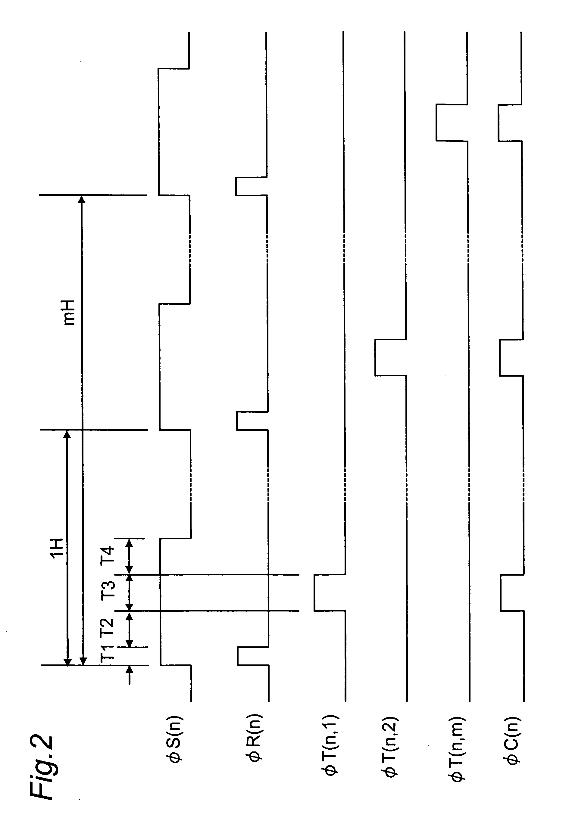
[0133]FIG. 8 shows drive timings in a case where the n-th line is the selected line. The description for this case is similar to that of the first embodiment and omitted.

[0134]FIG. 9 shows drive timings in a case where the n-t...


PUM


Abstract

An amplification type solid-state image pickup device of the invention includes a plurality of photoelectric conversion sections 10 each having an embedded photodiode 1 and a transfer transistor 2, a switched capacitor amplifier section 20 whose input side is connected to a charge detection node 8 to which output terminals of the plurality of photoelectric conversion sections 10 are connected in common, and a current amplification section 21 connected between the switched capacitor amplifier section 20 and a vertical signal line 9. Signal charge from the plurality of photoelectric conversion sections 10 is converted into voltage by the switched capacitor amplifier section 20, and the converted signal is current-amplified by the current amplification section 21 and outputted to the vertical signal line 9. Thus, a less-noise, high-quality image can be obtained while a reduction of the pixel size is achieved by reducing the number of transistors per pixel.

Description

CROSS-REFERENCE TO RELATED APPLICATIONS[0001]This nonprovisional application claims priority under 35 U.S.C. §119(a) on Patent Application No(s). 2007-022895 filed in Japan on Feb. 1, 2007, the entire contents of which are hereby incorporated by reference.BACKGROUND OF THE INVENTION[0002]The present invention relates to amplification type solid-state image pickup devices and, more particularly, to an amplification type solid-state image pickup device which includes a plurality of pixels each having a photoelectric conversion element and a transfer transistor for transferring signal charge of the photoelectric conversion element, in which signals from the pixels are amplified and outputted, respectively, to a signal line common to the pixels.[0003]Generally, there has been widely used an amplification type solid-state image pickup device which has a pixel section having an amplification function and a scanning circuit placed around the pixel section and in which pixel data are read f...

Claims


Application Information

Patent Timeline
IPC IPC(8): H03K19/14H01L27/146H04N5/335H04N5/341H04N5/357H04N5/369H04N5/374H04N5/3745H04N5/376
CPCH03K19/14H04N25/76
Inventor KOYAMA, EIJI
Owner SHARP KK
Why Eureka
Try Eureka