Semiconductor device and method of manufacturing semiconductor device

a semiconductor device and semiconductor technology, applied in the direction of semiconductor devices, electrical devices, transistors, etc., can solve the problems of difficult suppression of short channel effect, and achieve the effect of restrainting short channel effect and short channel

Inactive Publication Date: 2009-07-07
SONY CORP
View PDF7 Cites 18 Cited by
  • Summary
  • Abstract
  • Description
  • Claims
  • Application Information

AI Technical Summary

Benefits of technology

[0008]In the semiconductor device according the one embodiment of the present invention, the first epitaxial layer is so formed as to fill up the portion, cut out at the time of forming the side wall spacer, of the semiconductor substrate. Therefore, when the first epitaxial layer is formed to have an impurity concentration comparable to that of the semiconductor substrate, the semiconductor substrate is substantially restored into the state before being cut out, or the first epitaxial layer is formed to be above the surface of the semiconductor substrate. Besides, since the extension regions including the second epitaxial layer which is of a conduction type opposite to that of the first epitaxial layer and which is formed on the first epitaxial layer are provided, the extension regions are formed to be flush with the surface of the semiconductor substrate or to be above the surface, so that the short channel effect can be restrained.
[0009]The method of manufacturing a semiconductor device according to the another embodiment of the present invention includes the step of forming a first epitaxial layer so as to fill up the portion, cut out at the time of forming a side wall spacer, of a semiconductor substrate, so that the cut-out portion of the semiconductor substrate is filled up with the first epitaxial layer. In addition, when the first epitaxial layer is formed to have an impurity concentration comparable to that of the semiconductor substrate, the semiconductor substrate can be substantially restored into the state before being cut out, or the first epitaxial layer can be formed to be above the surface of the semiconductor substrate. Besides, since the manufacturing method includes the step of forming the extension regions including the second epitaxial layer which is of a conduction type opposite to that of the first epitaxial layer and which is formed on the first epitaxial layer, the extension regions are formed to be flush with the surface of the semiconductor substrate or to be above the surface, so that the short channel effect can be restrained.

Problems solved by technology

Thus, there is a need to solve the problem that, in the case of forming a side wall spacer of a silicon nitride film on only the side wall of a gate electrode on a silicon substrate, the silicon substrate would be cut out so as to make it difficult to form an elevated source / drain structure above the surface of the silicon substrate, which makes it difficult to suppress the short channel effect.

Method used


Image

  • Semiconductor device and method of manufacturing semiconductor device
  • Semiconductor device and method of manufacturing semiconductor device
  • Semiconductor device and method of manufacturing semiconductor device

Examples


example 1

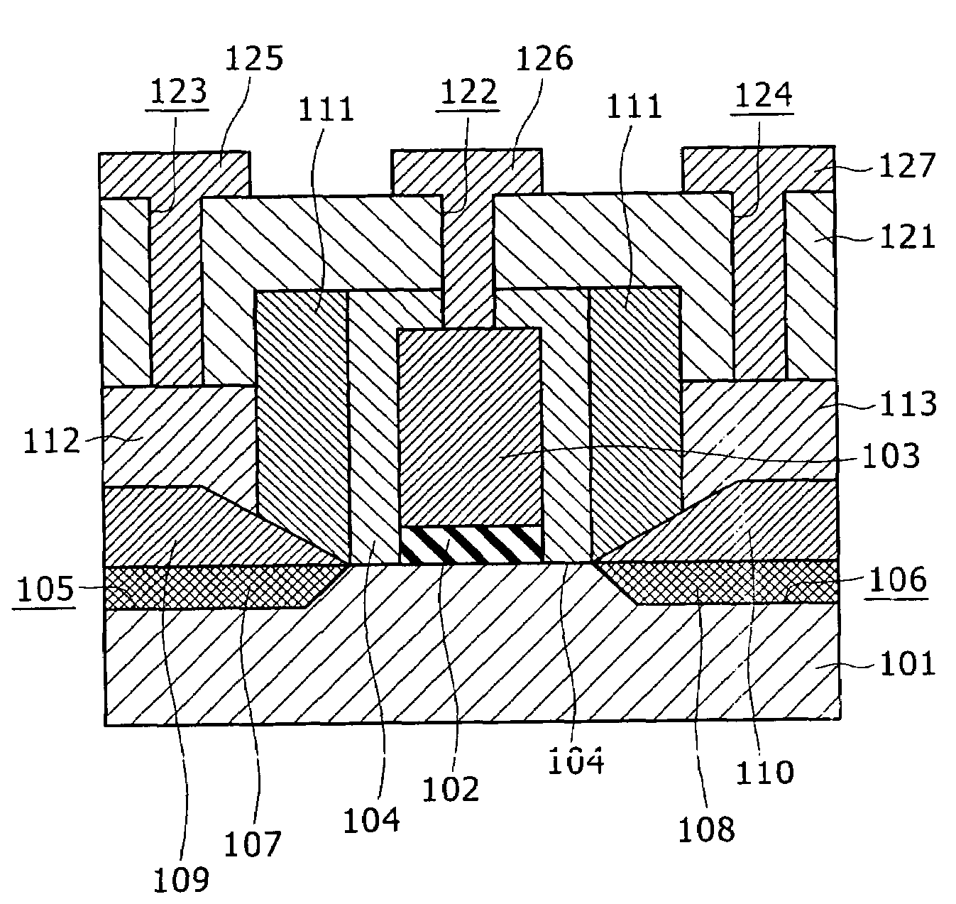
[0015]An example of the semiconductor device according to an embodiment of the present invention will be described referring to the schematic configuration sectional diagram shown in FIG. 1.

[0016]As shown in FIG. 1, a gate electrode 103 is formed on the upper side of a semiconductor substrate 101, with a gate insulation film 102 therebetween. A silicon substrate is used as the semiconductor substrate 101. As the semiconductor substrate 101, other substrates than the silicon substrate can also be used, for example, an SOI (Silicon on Insulator) substrate. The gate insulation film 102 can be composed of a silicon oxide film formed by a thermal oxidation process, for example, or can be composed of any of the dielectric films ordinarily used as a gate insulation film in MOS type transistors. The gate electrode 103 can be formed of polysilicon, for example.

[0017]A side wall spacer 104 is formed on the side wall of the gate electrode 103. The side wall spacer 104 is composed of a silicon ...

example 2

[0025]An example of the method of manufacturing a semiconductor device according to another embodiment of the present invention will be described referring to the manufacturing step sectional diagrams shown in FIGS. 3A to 3I.

[0026]As shown in FIG. 3A, a silicon substrate is used as a semiconductor substrate 101. As the semiconductor substrate 101, other substrates than the silicon substrate can also be used, for example, an SOI (Silicon on Insulator) substrate.

[0027]Next, as shown in FIG. 3B, a gate insulation film 102 is formed on the surface of the semiconductor substrate 101. The gate insulation film 102 can be formed by a thermal oxidation process, for example; here, as an example, the gate insulation film 102 was formed by oxidizing the surface of the semiconductor substrate 101.

[0028]Subsequently, as shown in FIG. 3C, a gate electrode forming film 131 and a hard mask layer 132 to be an etching mask at the timing etching the gate electrode forming film 131 are sequentially form...


PUM


Abstract

A semiconductor device includes a side wall spacer formed on the side surface of a gate electrode formed on the upper side of a semiconductor substrate with a gate insulation film therebetween, extension regions built up on the semiconductor substrate, and source / drain regions formed on the extension regions, wherein a first epitaxial layer is formed so as to fill up portions, cut out at the time of forming the side wall spacer, of the semiconductor substrate, and the extension regions are formed on the first epitaxial layer from a second epitaxial layer of a conduction type opposite to that of the first epitaxial layer.

Description

CROSS REFERENCES TO RELATED APPLICATIONS[0001]The present invention contains subject matter related to Japanese Patent Application JP 2005-050213 filed in the Japanese Patent Office on Feb. 25, 2005, the entire contents of which being incorporated herein by reference.BACKGROUND OF THE INVENTION[0002]The present invention relates to a semiconductor device and a method of manufacturing a semiconductor device such that it is easy to reduce the short channel effect.[0003]As a structure for reducing the short channel effect in a CMOS transistor, there have been proposed many elevated source / drain structures (see, for example, Japanese Patent Laid-Open Nos. 2004-95639, 2004-152973, and 2002-231942). In the structures described in the just-mentioned parent references, formation of an extension portion above the surface of a semiconductor substrate is disclosed, for suppressing the short channel effect. In other configurations than those using a polycrystalline silicon (see, for example, Ja...

Claims


Application Information

Patent Timeline
Patent Type & Authority Patents(United States)
IPC IPC(8): H01L21/336
CPCH01L29/66636H01L21/30608H01L29/41775H01L29/6656H01L29/66628
Inventor ANDO, ATSUHIRO
Owner SONY CORP
Why Eureka
Try Eureka