Layered chip package that implements memory device

a memory device and chip technology, applied in the field of layered chip packages, can solve the problems of increasing the cost of the layered chip package, affecting the high-speed operation of the circuit, and difficulty in reducing the distance between the electrodes, so as to increase the reliability of the wiring and facilitate the formation of wiring

Inactive Publication Date: 2009-07-07
HEADWAY TECH INC +1
View PDF11 Cites 35 Cited by
  • Summary
  • Abstract
  • Description
  • Claims
  • Application Information

AI Technical Summary

Benefits of technology

[0020]It is a first object of the present invention to provide a layered chip package that includes a plurality of chips stacked and that implements a memory device, the layered chip package allowing easy formation of wiring for establishing electrical connection between the chips and being capable of increasing the reliability of the wiring.
[0021]It is a second object of the present invention to provide an electronic component that includes a layered chip package including a plurality of chips stacked and that implements a memory device, the electronic component allowing easy formation of wiring for establishing electrical connection between the chips and being capable of increasing the reliability of the wiring.
[0034]According to the layered chip package of the present invention or the first or second electronic component of the present invention, the wiring disposed on at least one of the side surfaces of the main body serves to establish electrical connection between the plurality of chips stacked. Consequently, it is possible to easily form wiring for establishing electrical connection between chips and to increase the reliability of the wiring.

Problems solved by technology

The wire bonding method has a problem that it is difficult to reduce the distance between the electrodes so as to avoid contact between wires, and a problem that high resistances of the wires hamper a high-speed operation of a circuit.
Unfortunately, however, the through electrode method requires a large number of steps for forming the through electrodes in chips, and consequently increases the cost for the layered chip package.
Consequently, voids or keyholes are prone to occur in the through electrodes due to poor filling of the holes with metal, so that the reliability of wiring using the through electrodes tends to be reduced.
When the upper and lower chips are joined to each other at high temperatures, however, misalignment between the upper and lower chips can occur due to expansion and contraction of the chips, which often results in electrical connection failure between the upper and lower chips.
The through electrode method has a further problem that, if the plurality of chips stacked include one or more defective chips, it is difficult to replace the defective chip(s) with non-defective one(s).
This heating also melts solder between non-defective chips, and can thereby cause oxidation or flowing-out of the solder between the non-defective chips.
As a result, electrical connection failure can occur between the non-defective chips.
For this reason, according to the through electrode method, it is difficult to replace one or more defective chips, if included in the stack of a plurality of chips, with non-defective one(s).
This can result in a reduction in yield and an increase in cost for the layered chip package.
The manufacturing method disclosed in U.S. Pat. No. 5,953,588 involves a number of process steps and this raises the cost for the layered chip package.
This is also a factor that raises the cost for the layered chip package.
According to this multilayer module, however, it is impossible to increase the proportion of the area occupied by the electronic element in each active layer, and consequently it is difficult to achieve higher integration.
The high resistance of the wiring and the stray capacitance generated by the wiring hamper a high-speed operation of the memory device.
In the case of constructing a memory device by stacking a plurality of chips and carrying out inter-chip wiring using through electrodes, however, there arise the problems that it is not easy to form wiring using through electrodes and the reliability of the wiring formed using through electrodes tends to be reduced, as described previously.
In the case of constructing a large-capacity memory device, in particular, these problems become more significant because of the complexity of wiring.

Method used


Image

  • Layered chip package that implements memory device
  • Layered chip package that implements memory device
  • Layered chip package that implements memory device

Examples


first embodiment

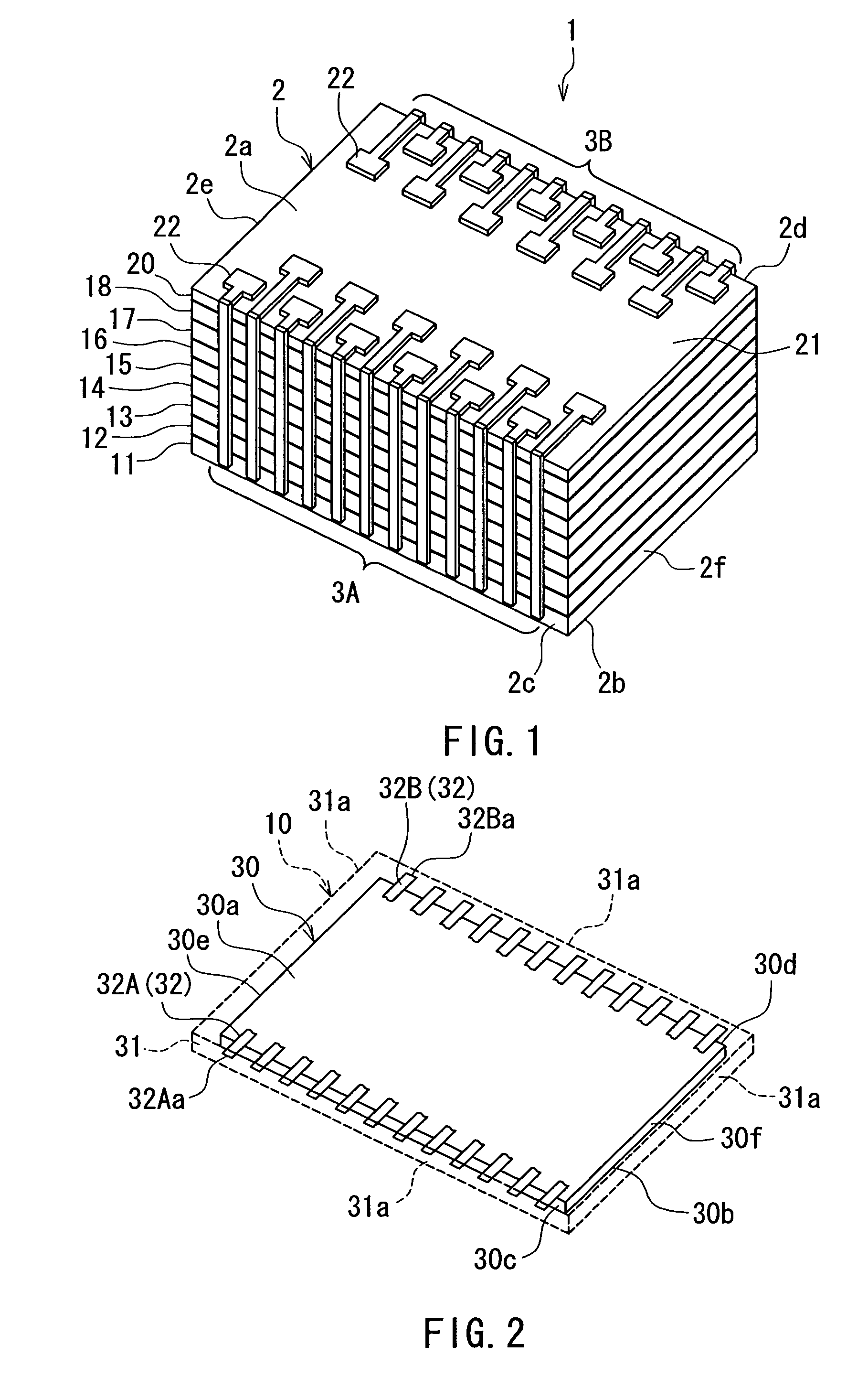
[0079]Embodiments of the present invention will now be described in detail with reference to the drawings. Reference is first made to FIG. 1 to describe the configuration of a layered chip package of a first embodiment of the invention. FIG. 1 is a perspective view of the layered chip package of the first embodiment. As shown in FIG. 1, the layered chip package 1 of the first embodiment includes a main body 2 that is rectangular-solid-shaped. The main body 2 has a top surface 2a, a bottom surface 2b, a first side surface 2c and a second side surface 2d facing toward opposite directions, and a third side surface 2e and a fourth side surface 2f facing toward opposite directions.

[0080]The layered chip package 1 further includes wiring disposed on at least one of the side surfaces of the main body 2. In the example shown in FIG. 1, the layered chip package 1 includes first wiring 3A disposed on the first side surface 2c of the main body 2, and second wiring 3B disposed on the second sid...

second embodiment

[0159]A second embodiment of the present invention will now be described. In the layered chip package 1 of the second embodiment, the four side surfaces 2c to 2f of the main body 2 include at least one first-type side surface on which the wiring 3 is disposed, and at least one second-type side surface on which the wiring 3 is not disposed. The appearance of the layered chip package 1 of the second embodiment is, for example, as shown in FIG. 1 as in the case of the first embodiment. In this example, of the four side surfaces 2c to 2f of the main body 2, the side surfaces 2c and 2d are the first-type side surfaces while the side surfaces 2e and 2f are the second-type side surfaces.

[0160]In the second embodiment, the four side surfaces 30c to 30f of the first-type or second-type semiconductor chip 30 include at least one first-type side surface that has the insulating portion 31 between itself and the at least one first-type side surface of the main body 2, and at least one second-typ...

third embodiment

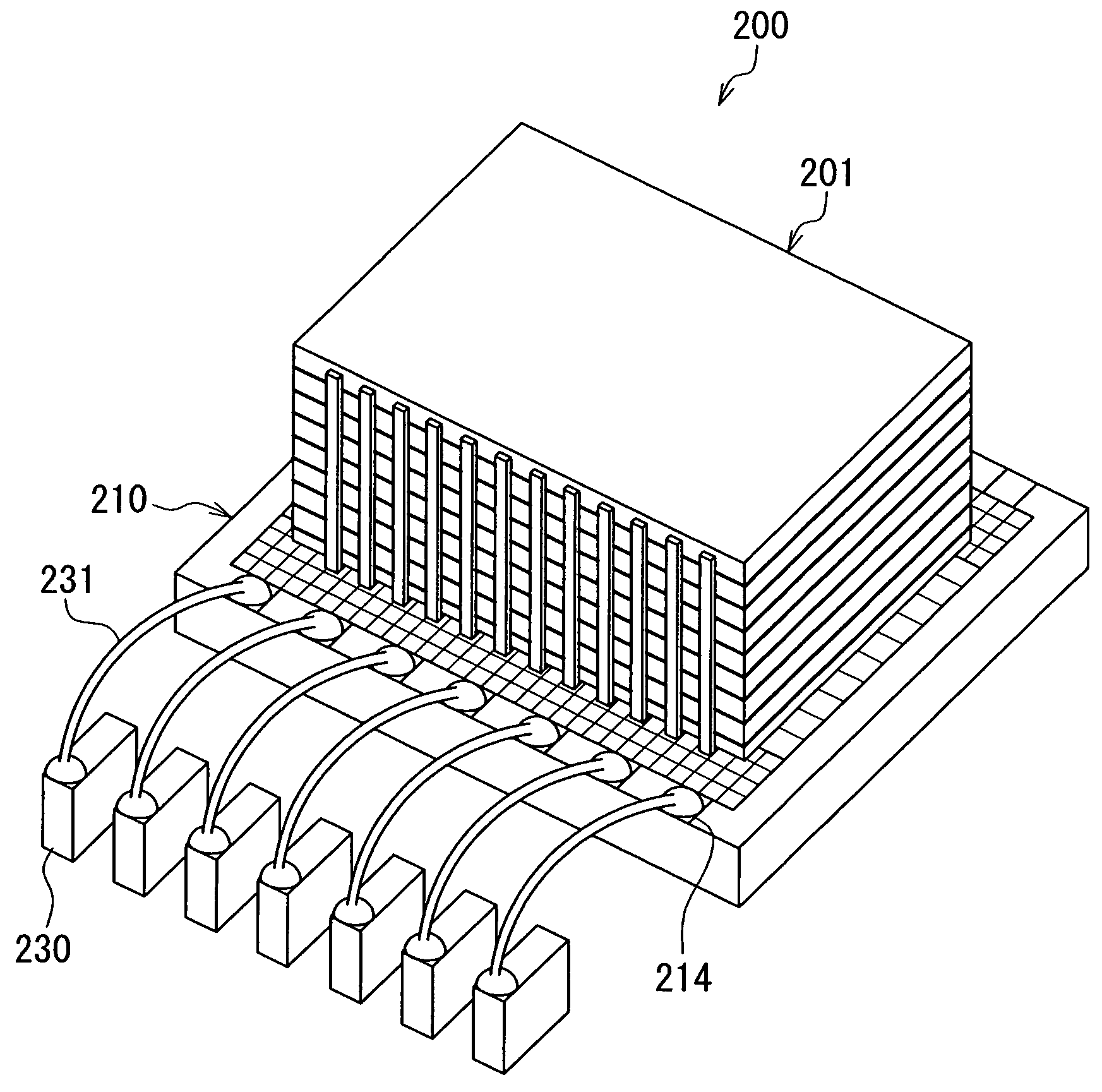
[0164]A third embodiment of the present invention will now be described. Reference is now made to FIG. 36 to describe the configuration of an electronic component of the third embodiment. FIG. 36 is a perspective view of the electronic component of the third embodiment. FIG. 37 is an exploded perspective view of the electronic component of FIG. 36. The electronic component of the third embodiment implements a memory device such as a flash memory, DRAM, SRAM, MRAM, PROM or FeRAM.

[0165]As shown in FIG. 36 and FIG. 37, the electronic component 200 of the present embodiment includes a layered chip package 201, and a circuit layer 210 bonded to the layered chip package 201. In the layered chip package 201 of the present embodiment, all the layer portions 10 included in the main body 2 are the first-type layer portions. In other words, all the layer portions 10 each include the first-type semiconductor chip 30. The first-type semiconductor chip 30 includes a plurality of memory cells. The...


PUM


Abstract

A layered chip package includes a main body, and wiring disposed on a side surface of the main body. The main body includes a plurality of first-type layer portions each including a first-type semiconductor chip; and a second-type layer portion including a second-type semiconductor chip. The first-type semiconductor chip includes a plurality of memory cells. The second-type semiconductor chip includes a control circuit that controls writing and reading on and from the memory cells included in the plurality of first-type layer portions. Each layer portion includes an insulating portion covering at least one side surface of the semiconductor chip, and a plurality of electrodes connected to the semiconductor chip. Each of the electrodes has an end face that is located at the side surface of the main body and connected to the wiring.

Description

BACKGROUND OF THE INVENTION[0001]1. Field of the Invention[0002]The present invention relates to a layered chip package that includes a plurality of chips stacked and that implements a memory device, and to an electronic component that includes a layered chip package including a plurality of chips stacked and that implements a memory device.[0003]2. Description of the Related Art[0004]In recent years, a reduction in weight and an improvement in performance have been demanded of mobile devices typified by cellular phones and notebook personal computers. Accordingly, there has been a demand for higher integration of electronic components for use in mobile devices. Higher integration of electronic components has been demanded also for achieving an increase in capacity of semiconductor memory.[0005]As an example of highly integrated electronic components, a system-in-package (hereinafter referred to as SiP), especially an SiP utilizing a three-dimensional packaging technology for stacki...

Claims


Application Information

Patent Timeline
Patent Type & Authority Patents(United States)
IPC IPC(8): H01L23/02H01L23/48H01L23/52H01L29/40
CPCH01L21/6835H01L23/544H01L24/24H01L24/25H01L24/48H01L24/73H01L24/82H01L24/94H01L24/96H01L25/0657H01L25/105H01L25/18H01L25/50H01L25/16H01L2924/07802H01L2924/10253H01L2225/1011H01L2225/06524H01L2225/1058H01L2221/68359H01L2223/5442H01L2223/54426H01L2224/16H01L2224/18H01L2224/48091H01L2224/48464H01L2224/49175H01L2224/4943H01L2225/06513H01L2225/06551H01L2924/01004H01L2924/01014H01L2924/01015H01L2924/01029H01L2924/01075H01L2924/01078H01L2924/01082H01L2924/014H01L2924/30105H01L2924/01006H01L2924/01033H01L24/49H01L2924/00014H01L2924/00H01L2924/181H01L2224/24137H01L2224/73267H01L2224/45099H01L2224/05599
Inventor SASAKI, YOSHITAKAITO, HIROYUKIHARADA, TATSUYAOKUZAWA, NOBUYUKISUEKI, SATORUHASHIMOTO, RYUJI
Owner HEADWAY TECH INC
Why Eureka
Try Eureka