Stacked chip security

a technology of stacked chips and security, applied in the direction of semiconductor/solid-state device testing/measurement, semiconductor/solid-state device details, instruments, etc., can solve the problem of slow communication speed, and achieve the effect of providing signal security through stacked multi-chip approaches

Inactive Publication Date: 2009-07-07
INT BUSINESS MASCH CORP
View PDF18 Cites 225 Cited by
  • Summary
  • Abstract
  • Description
  • Claims
  • Application Information

AI Technical Summary

Problems solved by technology

In other words, the larger the separation distance between two circuit components, the slower the speed at which they are able to communicate.
However, one drawback to the stacked multi-chip approach relates to providing signal security.

Method used


Image

  • Stacked chip security
  • Stacked chip security
  • Stacked chip security

Examples


Embodiment Construction

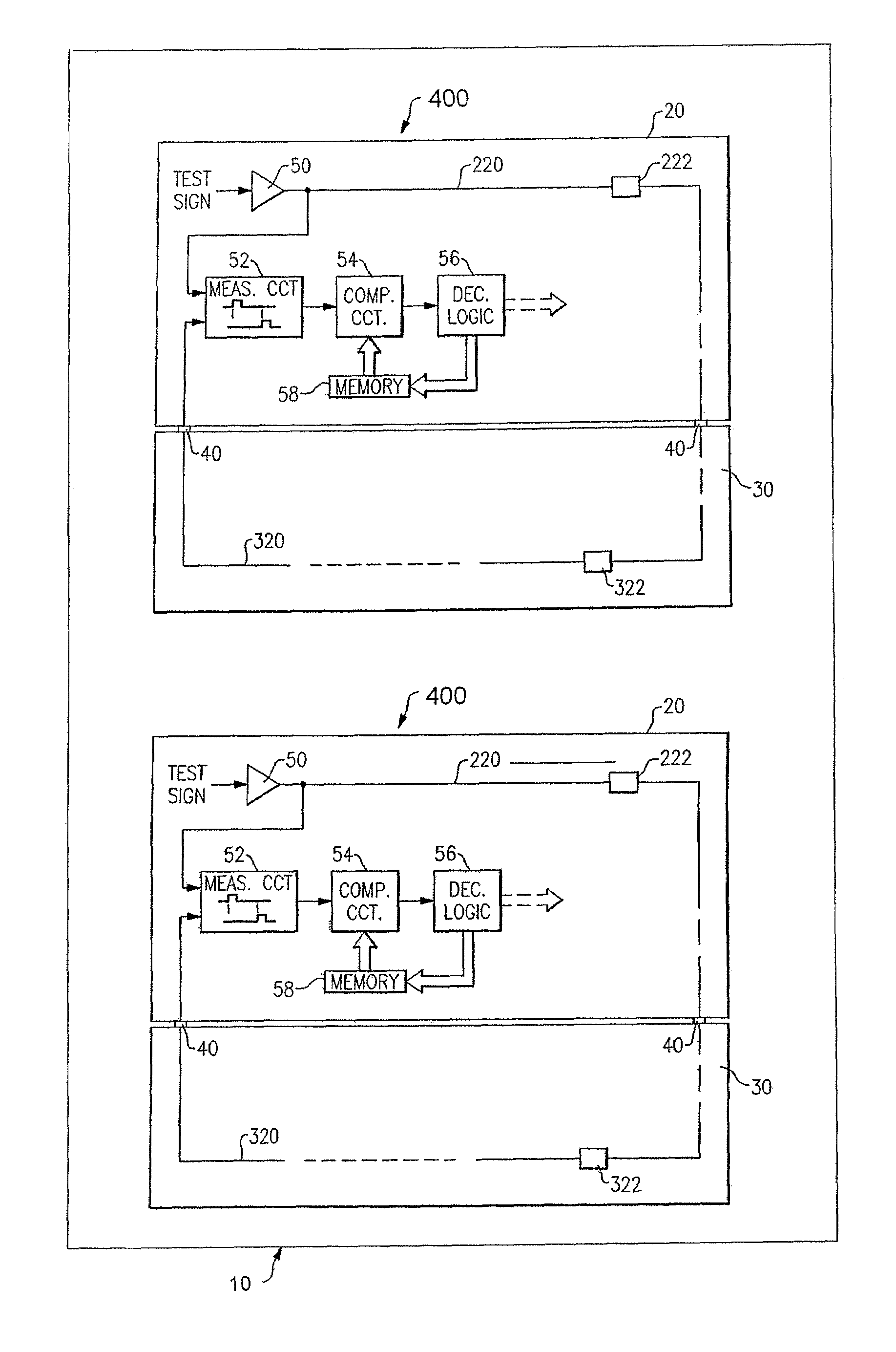
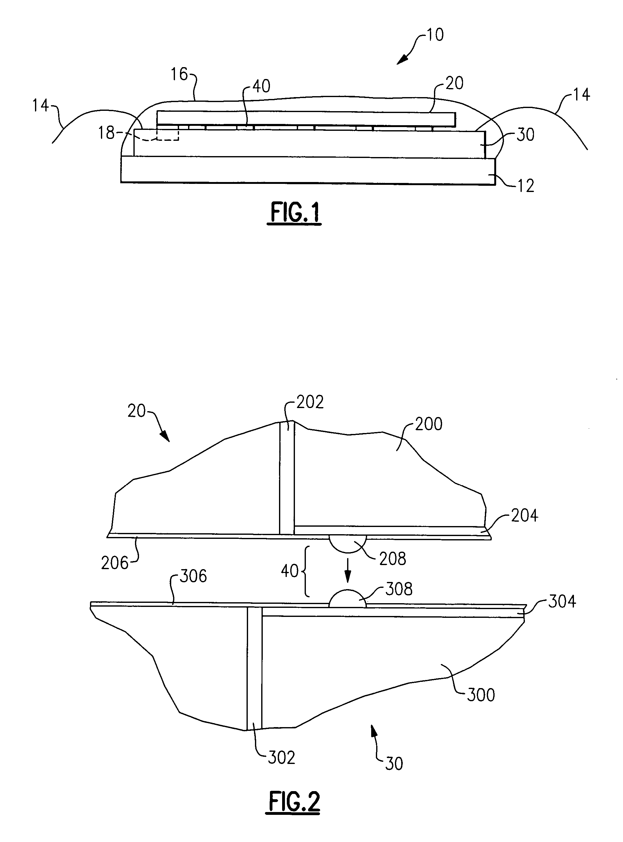
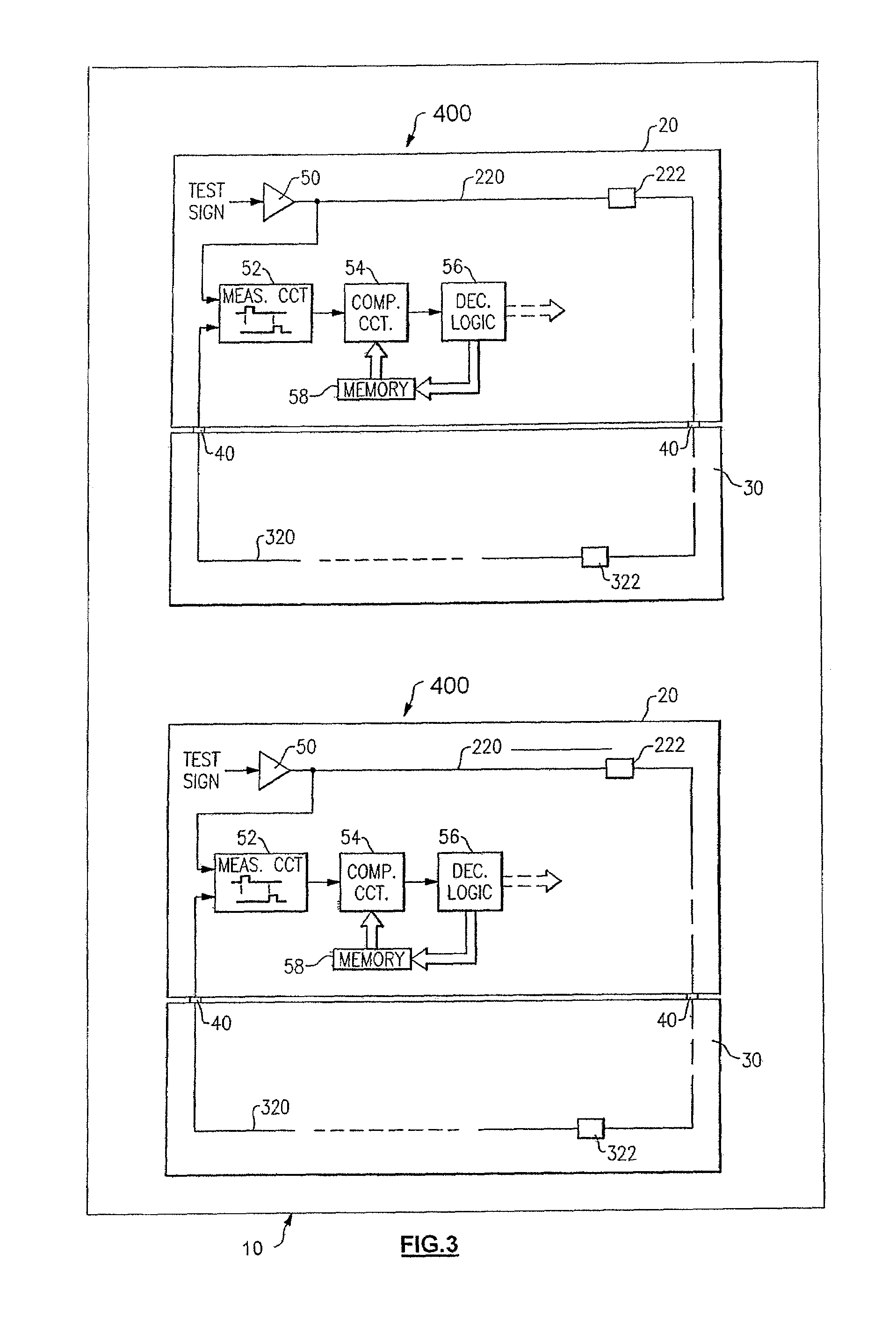
[0018]Reference will now be made in detail to the present exemplary embodiments of the invention, examples of which are illustrated in the accompanying drawings. Wherever possible, the same reference numbers will be used throughout the drawings to refer to the same or like parts. An embodiment of the integrated circuit module of the present invention is shown in FIG. 1, and is designated generally throughout by reference numeral 10.

[0019]As embodied herein, and depicted in FIG. 1, a sectional view of an integrated circuit module 10 in accordance with one embodiment of the present invention is shown. Module 10 includes a semiconductor chip 20. Chip 20 is coupled to another semiconductor chip 30 by way of interconnections 40. A capacitor circuit 18 may be disposed between chip 20 and chip 30. If an attempt is made to separate chip 20 from chip 30, the capacitor is discharged and module 10 is disabled. Capacitor 18 may be charged during device programming. The device is configured such...


PUM


Abstract

The present invention is directed to an integrated circuit module device. The device includes a first semiconductor chip having a first circuit layer and at least one first interconnection element disposed on a first chip surface. The at least one first interconnection element is electrically coupled to the first circuit layer. A second semiconductor chip includes a second circuit layer and at least one second interconnection element disposed on a second chip surface. The at least one second interconnection element is electrically coupled to the second circuit layer. The at least one first interconnection element is connected to the at least one second interconnection element to establish electrical continuity between the first circuit layer and the second circuit layer. The first surface is adjoined to the second surface. At least one ring delay circuit includes a first ring delay path partially disposed on the first circuit layer and a second ring delay path partially disposed on the second circuit layer. The first ring delay path and the second ring delay path form a signal path having a predetermined measurement signature. The ring delay circuit compares the predetermined measurement signature to a test measurement signature.

Description

BACKGROUND OF THE INVENTION[0001]1. Field of the Invention[0002]The present invention relates generally to semiconductor devices, and particularly to integrated circuit modules.[0003]2. Technical Background[0004]Integrated circuits are thin semiconductor chips that include a large number of semiconductor devices, i.e., transistors and resistors, disposed thereon. A typical semiconductor chip may have a surface area of approximately 10 mm2 to 600 mm2. Examples of integrated circuits include microprocessors, signal processors, and volatile and non-volatile memory devices.[0005]Integrated circuits are fabricated by various steps that result in a circuit layer being disposed on a semiconductor wafer. The wafer may be comprised of silicon, gallium arsenide, or other such materials. For example, in some special applications, a substrate is formed by disposing silicon on sapphire. Photolithographic techniques are used to pattern the wafer. Repeated steps of deposition, patterning and etchi...

Claims


Application Information

Patent Timeline
Patent Type & Authority Patents(United States)
IPC IPC(8): G01R31/02
CPCH01L23/576H01L23/585H01L25/0657H01L24/48H01L2224/16145H01L2224/48227H01L2225/06568H01L2224/81203H01L2224/81815H01L2225/0651H01L2924/1431H01L2924/1434H01L2225/06513H01L2224/81193H01L2224/8592H01L2924/00011H01L2924/00014H01L2924/14H01L2924/00H01L2224/0401H01L2224/45099H01L2224/45015H01L2924/207
Inventor ANDERSON, BRENT ALANSPROGIS, EDMUND JURIS
Owner INT BUSINESS MASCH CORP
Why Eureka
Try Eureka