
Receiver of high speed digital interface

a digital interface and receiver technology, applied in the field of receivers of high-speed digital interfaces, can solve the problems of reducing dc offset and detrimentally saturating differential output signals with invalid information, and achieve the effect of reducing dc offset and improving impedance matching

Inactive Publication Date: 2009-07-14
HIMAX TECH LTD
View PDF3 Cites 12 Cited by
  • Summary
  • Abstract
  • Description
  • Claims
  • Application Information

AI Technical Summary

Benefits of technology

The invention provides a receiver for a high-speed digital interface with a limiting amplifier that reduces DC offset and improves impedance matching. The receiver includes a differential amplifier, resistive elements, transistors, and low-pass filters. The transistors have drains coupled to the input terminals of the differential amplifier and a reference voltage, and the sources of the transistors receive a common mode voltage. The resistive elements have one end coupled to the input terminals of the differential amplifier and the other end receiving a reference voltage. The low-pass filters receive the amplified differential signal and derive a differential feedback signal. The transistors have drains coupled to the input terminals of the differential amplifier and the sources of the transistors receive a bias voltage. The invention also provides a receiver with improved impedance matching and reduced DC offset.

Problems solved by technology

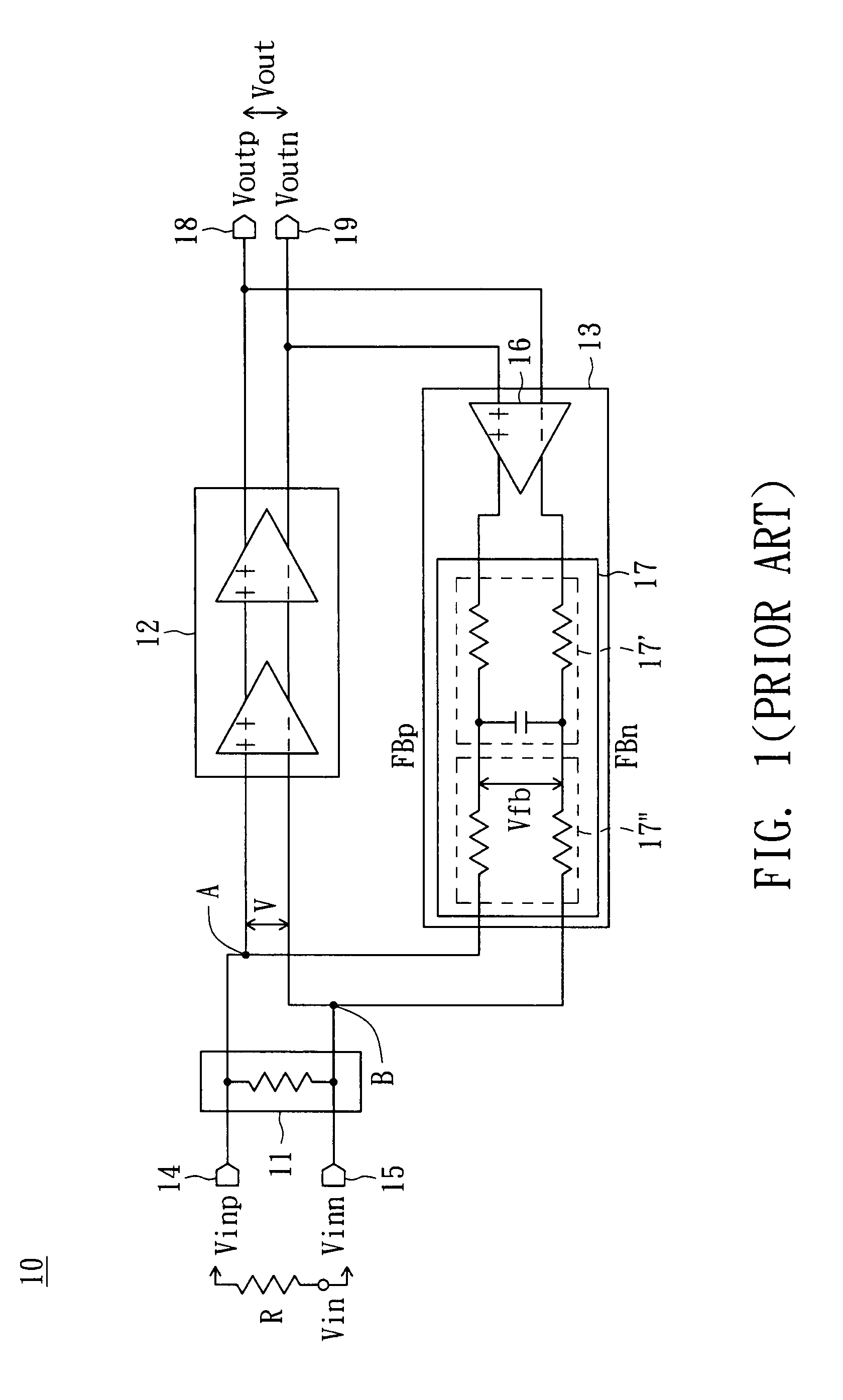
The conventional differential amplifier shown in FIG. 1 only partially reduces the DC offset, because, unfortunately, it amplifies not only the useful input signal but also any DC offset signal, coming from the previous circuits or internally generated at the input terminals of amplifier 10.
The amplitude of this DC offset signal can be of the same order of magnitude or even greater than the one of the input signal itself and then can detrimentally saturate the differential output signal with invalid information.

Method used


Image

  • Receiver of high speed digital interface
  • Receiver of high speed digital interface
  • Receiver of high speed digital interface

Examples


Embodiment Construction

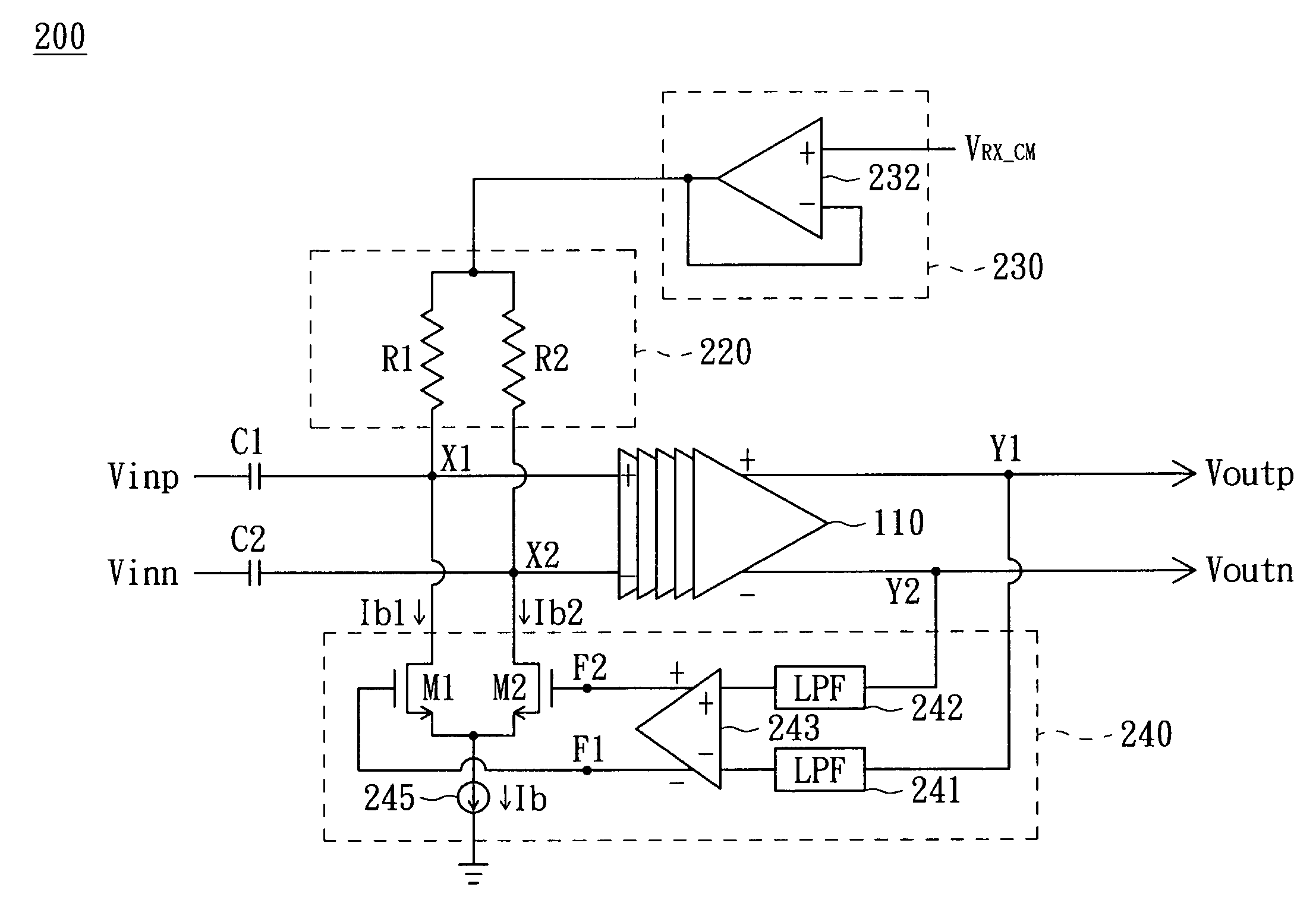
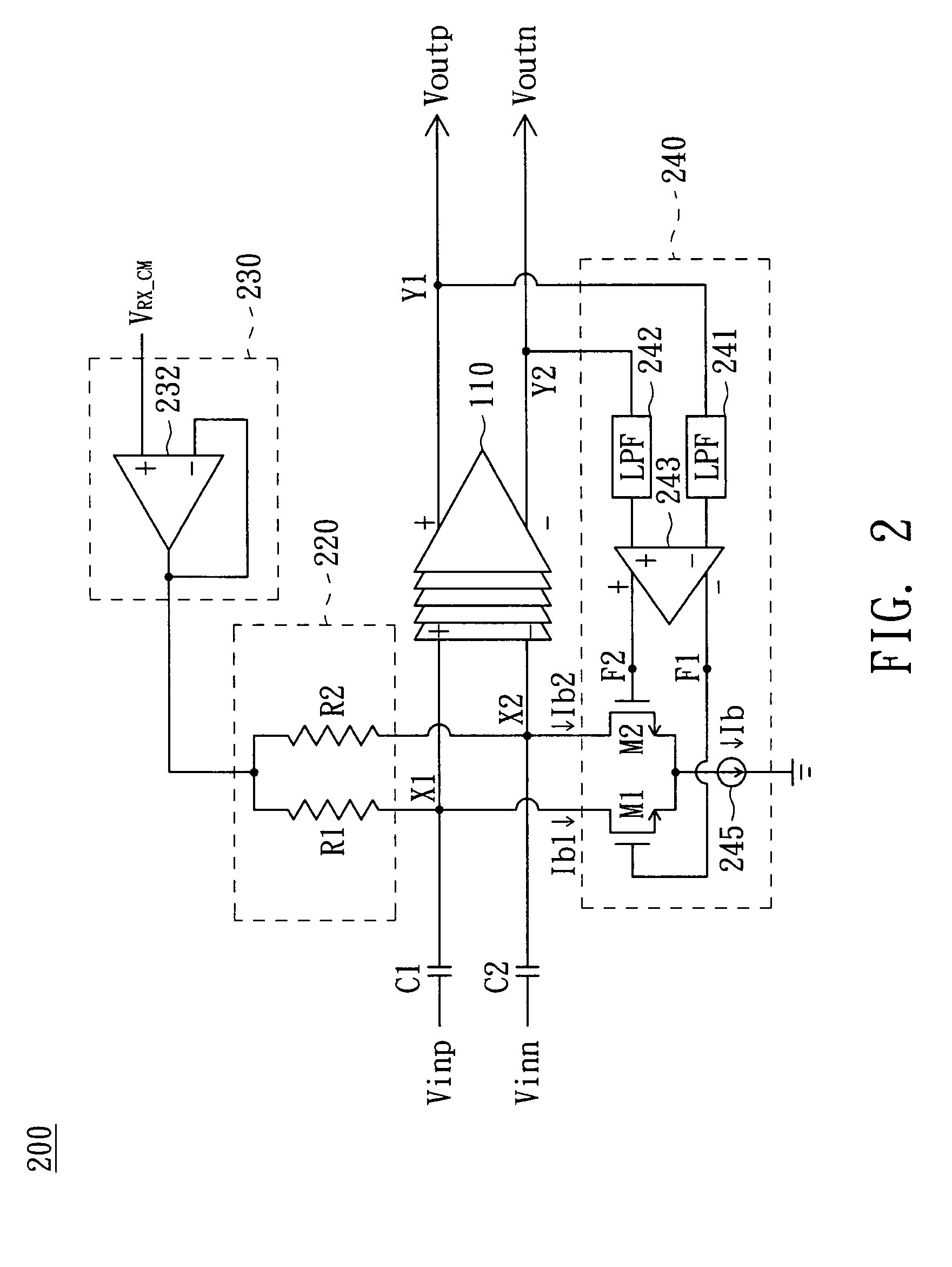
[0017]FIG. 2 is a general block diagram showing a receiver 200 of a high speed digital interface according to a preferred embodiment of the invention. The receiver 200 includes at least one differential amplifier 210, a resistive matching circuit 220, an input common mode bias circuit 230 and an offset cancellation circuit 240.

[0018]The differential amplifier 210 may be a single differential amplifier or may be composed of multiple stages. The differential amplifier 210 has a first input terminal X1, a second input terminal X2, a first output terminal Y1 and a second output terminal Y2. The first input terminal X1 and the second input terminal X2 are respectively coupled to a first capacitance C1 and a second capacitance C2. The differential amplifier 210 receives a small differential signal (Vinp, Vinn) in an AC-coupled manner, wherein the first input terminal X1 receives a positive input signal Vinp, and the second input terminal X2 receives a negative input signal Vinn. The diffe...


PUM


Abstract

A receiver of a high speed digital interface includes at least one differential amplifier, a pair of resistive elements, a current source and a pair of transistors. The differential amplifier receives a small differential signal at a pair of input terminals and outputs an amplified differential signal. Each of the resistive elements has one end coupled to one of the input terminals of the differential amplifier and the other end receiving a reference voltage. The pair of transistors has drains respectively coupled to the input terminals of the differential amplifier, sources commonly coupled to the current source and gates receiving a differential feedback signal derived from the amplified differential signal.

Description

BACKGROUND OF THE INVENTION[0001]1. Field of the Invention[0002]The present invention relates in general to a receiver of a high speed digital interface, and more particularly to a receiver having a limiting amplifier with reduced DC offset and improved impedance matching.[0003]2. Description of the Related Art[0004]In a receiver side of a high speed digital interface, there is a need for the amplification of high frequency low power signals. This is achieved with a dedicated differential amplifier basically consisting of a chain of low gain large bandwidth amplifiers with a parallel feedback loop.[0005]Referring to FIG. 1, a block diagram of a conventional limiting differential amplifier in a receiver side of a high speed digital interface is shown. The differential amplifier 10 includes an input matching circuit 11, an amplification section 12 and a feedback block 13. The amplification section 12 consists of a chain of large bandwidth amplifiers to obtain enough gain in the freque...

Claims


Application Information

Patent Timeline
Patent Type & Authority Patents(United States)
IPC IPC(8): H03L5/00H03K5/08
CPCH03F3/45475H03F3/45968H03F2203/45134H03F2203/45138H04L25/0292H03F2203/45521H03F2203/45544H03F2203/45588H04L25/0272H03F2203/45212
Inventor CHU, YUAN-KAI
Owner HIMAX TECH LTD
Learn More