Solid-state image pickup device

a solid-state image and pickup device technology, applied in the field of solid-state image pickup devices, can solve the problems of difference in output range between and increase in output voltage, and achieve the effects of reducing load on an external system, reducing output voltage, and reducing output voltag

Inactive Publication Date: 2009-07-14
CANON KK
View PDF15 Cites 38 Cited by
  • Summary
  • Abstract
  • Description
  • Claims
  • Application Information

AI Technical Summary

Benefits of technology

[0010]It is possible to maintain the same output range at the time of adding a plurality of pixel signals and at the time of not adding pixel signals, and maintain the same dynamic range in both cases. This eliminates the need to provide an arithmetic operation unit outside the solid-state image pickup device, for maintaining an output amplitude range at the time of addition and an output amplitude range at the time of non-addition to coincide with each other, and thereby makes it possible to reduce load on an external system.
[0011]The solid-state image pickup device according to the present invention can make the dynamic range at the time of addition to be the same as that at the time of non-addition at higher precision.

Problems solved by technology

However, in the solid-state image pickup device of the above described patent document, if the number of pixels to be added increases, the amount of charge accumulated in a memory 16 increases, thus resulting in an increase in output voltage.
This causes the problem of difference in output range between at the time of addition and at the time of non-addition.

Method used


Image

  • Solid-state image pickup device
  • Solid-state image pickup device
  • Solid-state image pickup device

Examples


first embodiment

[0022]A solid-state image pickup device according to the first embodiment of the present invention will be described below. This embodiment will describe a case of vertical two-pixel summation.

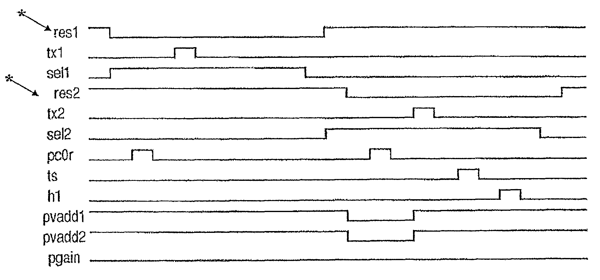
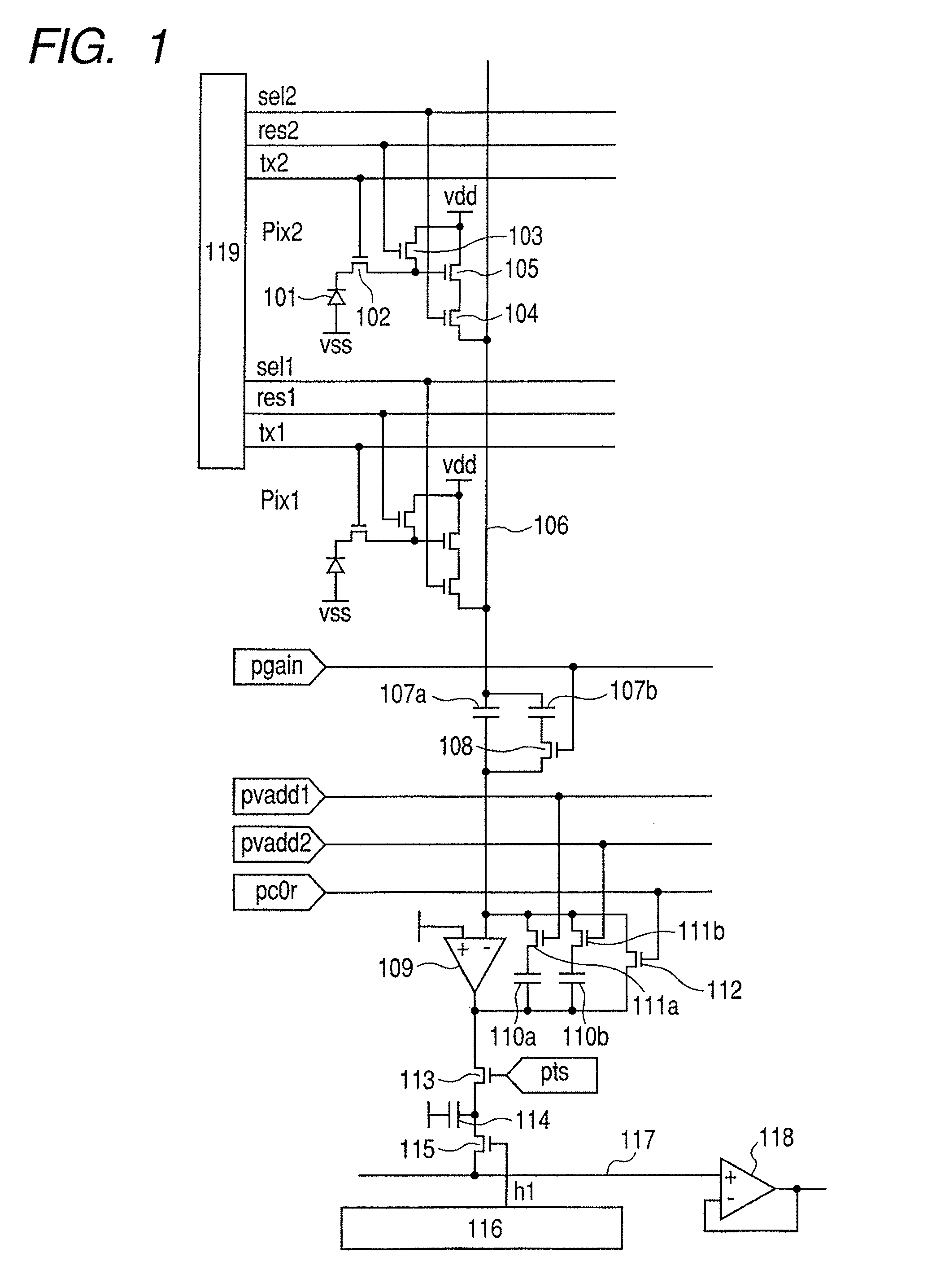
[0023]FIG. 1 is a diagram of an equivalent circuit of the solid-state image pickup device of the first embodiment and shows a part associated with 2×1 pixels of two-dimensionally arrayed pixels. A unit pixel has a photodiode 101 which is a photoelectric conversion element, an amplifying MOSFET 105 which amplifies a signal corresponding to the electrical charge generated by photoelectric conversion at the photodiode 101, and a switch 102 which transfers charge generated at the photodiode 101 to a gate electrode of the amplifying MOSFET 105. The unit pixel also has a reset switch 103 which resets a gate electrode of the amplifying MOSFET 105 to a predetermined voltage and a row selection switch 104 which controls electrical continuity between a source electrode of the amplifying MOSFET 105 and a...

second embodiment

[0032]A solid-state image pickup device according to the second embodiment of the present invention will be described below. This embodiment will describe a case of vertical three-pixel addition.

[0033]FIG. 4 is a diagram of an equivalent circuit of the solid-state image pickup device of the second embodiment and shows a part associated with 3×1 pixels of two-dimensionally arrayed pixels. An explanation of the components denoted by the same reference numerals as those in FIG. 1 will be omitted.

[0034]Since the second embodiment performs three-pixel addition, the capacitance value of a clamp capacitor element can be set to 1 or ⅓ of the capacitance value of a feedback capacitor element by controlling the clamp capacitor changeover switch 108.

[0035]Readout methods in a non-adding mode and in an adding mode will be explained next. Assume that capacitance value of capacitors 107a and 107b are (⅔)×C0 and ( 4 / 3)×C0 respectively, and that capacitors 110a and 110b each have a capacitance valu...

third embodiment

[0040]A solid-state image pickup device according to the third embodiment of the present invention will be described below. This embodiment will describe a case where vertical two pixels are added in a floating diffusion (to be referred to as FD hereinafter) unit.

[0041]FIG. 6 is a diagram of an equivalent circuit of the solid-state image pickup device of the third embodiment and shows a part associated with 2×1 pixels of two-dimensionally arrayed pixels. An explanation of the components denoted by the same reference numerals as those in FIG. 1 will be omitted. As for pixels in this embodiment, two pixels share the FD unit. A unit pixel has photodiodes 601a and 601b, switches 602 and 603 which transfer charge generated at the photodiodes 601a and 601b to the gate electrode of an amplifying MOSFET 605 serving as a detection unit, and the amplifying MOSFET 605, which amplifies a signal generated at each of the photodiodes 601a and 601b. The unit pixel also has a reset switch 604 which ...


PUM


Abstract

There is provided a solid-state image pickup device comprising a plurality of pixel units, each of which includes a photoelectric conversion element, a signal line which reads out signals from said plurality of pixel units, a first capacitor element which has a first electrode connected to the signal line, an amplifier which has an input terminal connected to a second electrode of the first capacitor element, and a second capacitor element connected between the input terminal and an output terminal of the amplifier, wherein the first capacitor element has a capacitance value which is smaller at the time of execution of an adding mode than at the time of execution of a non-adding mode, and thereby making an amplification factor of the amplifier smaller at the time of execution of the adding mode than at the time of execution of the non-adding mode.

Description

BACKGROUND OF THE INVENTION[0001]1. Field of the Invention[0002]The present invention relates to a solid-state image pickup device, particularly to a solid-state image pickup device used in a scanner, video camera, digital still camera or the like.[0003]2. Description of the Related Art[0004]In recent years, there have been available image input apparatuses such as a digital camera, video camera and image reader. A CCD image sensor or a solid-state image pickup device called non-CCD image sensor such as a bipolar transistor image sensor, FET image sensor or CMOS image sensor are provided in an image input apparatus. A solid-state image pickup device converts optical image information into electrical signals. The obtained electrical signals are subjected to various types of signal processing and displayed on a display or recorded on a storage medium.[0005]Solid-state image pickup devices of today which use an amplifying MOS sensor generally adopt progressive scanning, which scans eac...

Claims


Application Information

Patent Timeline
Patent Type & Authority Patents(United States)
IPC IPC(8): H04N3/14H04N5/335H04N5/347H04N5/355H04N5/378
CPCH04N3/155H04N5/378H04N5/355H04N5/347H04N25/42H04N25/46H04N25/57H04N25/75
Inventor NODA, TOMOYUKIINUI, FUMIHIROTAKAHASHI, HIDEKAZU
Owner CANON KK
Why Eureka
Try Eureka