Method for mounting semiconductor chips, and corresponding semiconductor chip system

a technology of semiconductor chips and mounting methods, applied in the direction of semiconductor devices, instruments, measurement devices, etc., can solve problems such as gel damage, and achieve the effects of high mechanical strength, simple and cost-effective configuration, and cost-effectiveness

Inactive Publication Date: 2009-07-21
ROBERT BOSCH GMBH
View PDF9 Cites 11 Cited by
  • Summary
  • Abstract
  • Description
  • Claims
  • Application Information

AI Technical Summary

Benefits of technology

[0020]An example method according to the present invention for mounting semiconductor chips and a corresponding semiconductor chip system may have the advantage over conventional approaches that they allow a simple and cost-effective configuration, which is not susceptible to stressing.
[0021]An example embodiment of the present invention may also have the advantage that, compared to an absolute-pressure sensor without a second pressure connection, no further process steps are required apart from an additional, brief silicon trenching step to open an access opening to a cavity, thereby making the example method according to the present invention very cost-effective. The etching step for opening the second pressure access need not be implemented through the entire sensor, but only through a slight thickness of the diaphragm, which requires a short etching process.
[0023]A monocrystalline silicon diaphragm is able to be produced whose special advantage is the high mechanical strength and the high K factor of the piezoresistors doped therein.
[0024]Solder connecting on the semiconductor chip and the substrate brings about alignment of the semiconductor chip due to the surface tension of the solder. The energetically most advantageous state may be attained when the solder between two contact surfaces on chip and substrate has the smallest surface. This may be achieved when both areas are positioned directly on top of one another. With the aid of this self-adjustment the pressure access hole is precisely adjusted on the chip connection. This may allow a precise alignment even of very small structures.
[0026]Electrical preliminary measuring in the wafer composite is possible, as is an adjustment at the end of production line after mounting on the carrier. The example method according to the present invention may also allow a space-saving configuration of sensor chip and evaluation circuit.

Problems solved by technology

However, such a configuration has the disadvantage that it is cumbersome and that problems frequently arise with the hermetic enclosing of sensor chip 5, for instance because of leaky welding seams or the like.
When such a gel 2 is used, the maximum pressure is disadvantageously determined by gel 2, since gas diffuses into gel 2 and, if there is a sudden reduction in pressure, gas bubbles are created in gel 2, which destroy gel 2.

Method used


Image

  • Method for mounting semiconductor chips, and corresponding semiconductor chip system
  • Method for mounting semiconductor chips, and corresponding semiconductor chip system
  • Method for mounting semiconductor chips, and corresponding semiconductor chip system

Examples


Embodiment Construction

[0048]In the figures, like reference numerals designate like or functionally equivalent components.

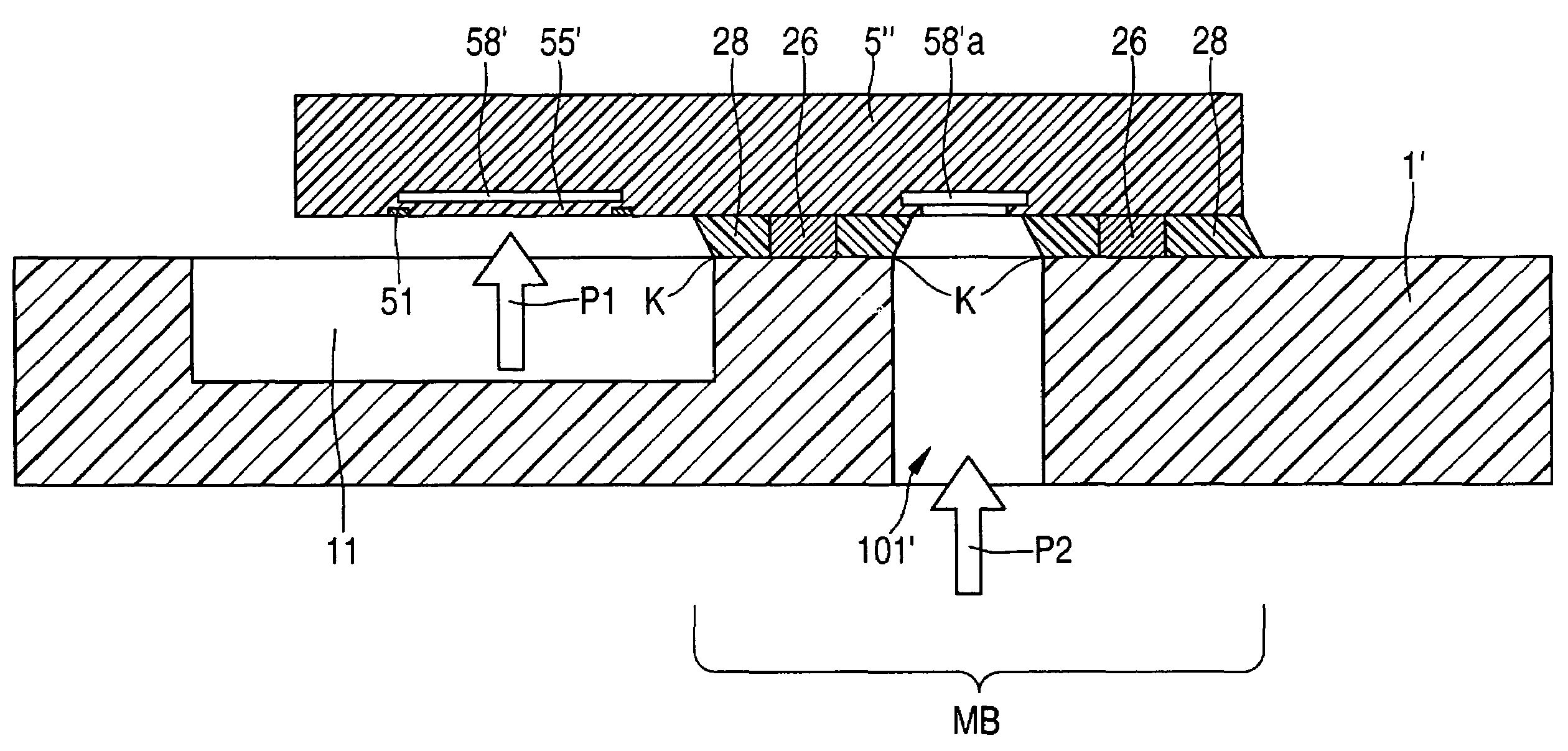
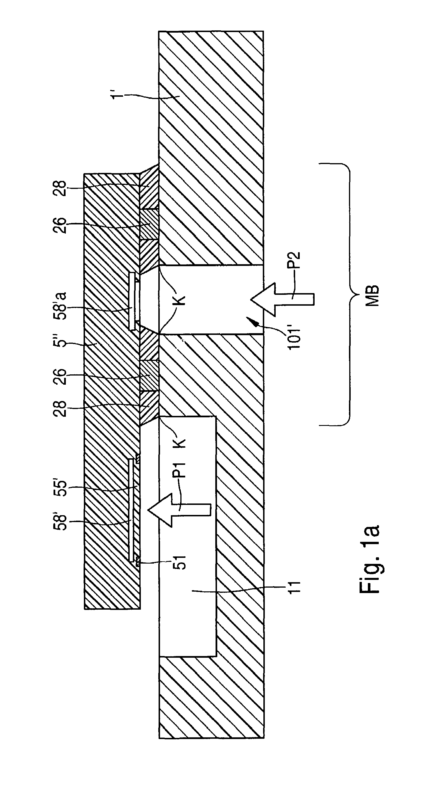
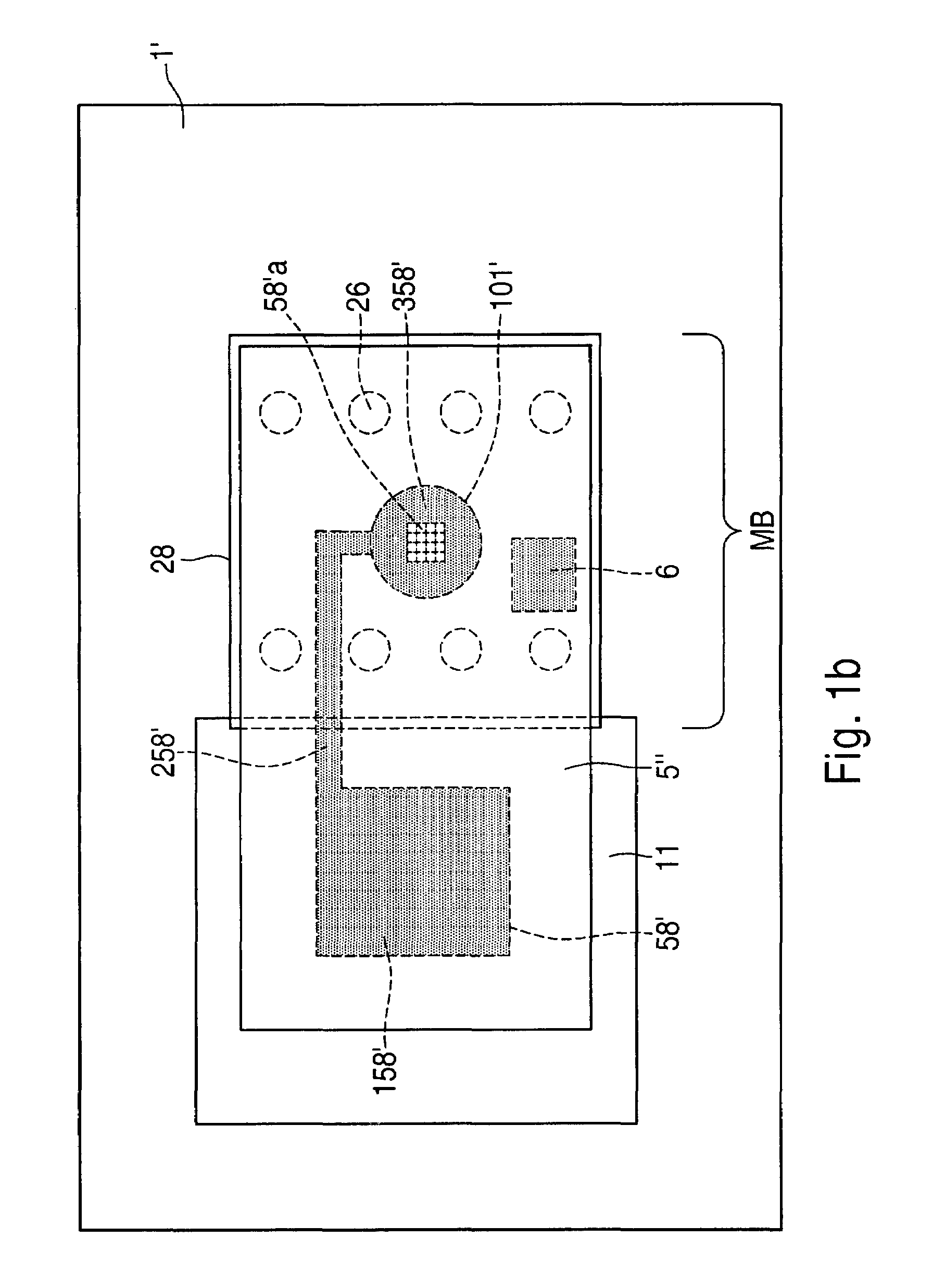
[0049]FIGS. 1a,b show a first specific example embodiment of the method according to the present invention for mounting semiconductor chips and a corresponding semiconductor chip system in a side view and a plane cross-sectional view.

[0050]In this example, sensor chip 5″ is a surface-micromechanical sensor chip, which was produced according to the method described in German Patent Application No. DE 100 32 579 A1, for example, and which has an integrated cavity 58′ above a diaphragm region 55′.

[0051]For mounting, bond pads of sensor chip 5″ are soldered to bond pads (not shown) of substrate 1′ in a mounting region MB using a solder or bonding connection, such as solder balls 26, the substrate in this case being a printed circuit board or ceramic and having a recess 11 next to which sensor chip 5″ is mounted in flip-chip technology, so as to overhang.

[0052]In addition, mounting region M...


PUM


Abstract

A method is described for mounting semiconductor chips and a corresponding semiconductor chip system. The method may include providing a semiconductor chip having a surface that includes a diaphragm region and a peripheral region, the peripheral region having a mounting region, and a cavity being disposed underneath the diaphragm region, which extends into the mounting region and ends there in an opening. The method may also include providing a substrate which has a surface having a recess; mounting the mounting region of the semiconductor chip in flip-chip technology onto the surface of the substrate in such a way that an edge of the recess lies between the mounting region and the diaphragm region and the opening faces in the direction of the substrate. Additionally, the mounting region is underfilled using an underfilling, the edge of the recess serving as separating region for the underfilling so that no underfilling reaches the diaphragm region; and a through hole is provided through the substrate to the opening of the cavity.

Description

FIELD OF THE INVENTION[0001]The present invention relates to a method for mounting semiconductor chips and to a corresponding semiconductor chip system. Although applicable to any semiconductor chip system, the present invention as well as the problem underlying it are explained with respect to a micromechanical semiconductor chip system having a pressure sensor.BACKGROUND INFORMATION[0002]German Patent Application No. DE 102 004 011 203 describes various examples of methods for mounting semiconductor chips and corresponding semiconductor chip systems of which three examples will be discussed in greater detail in the following text.[0003]FIG. 7 shows a first example for a method of mounting semiconductor chips and a corresponding semiconductor chip system in a cross-sectional view.[0004]In FIG. 7, reference numeral 100 denotes a TO8 base produced from Kovar, for example. Reference numeral 5 is a micromechanical silicon pressure sensor chip having piezoresistive transducer elements 5...

Claims


Application Information

Patent Timeline
Patent Type & Authority Patents(United States)
IPC IPC(8): H01L21/00
CPCG01L9/0054G01L19/0038G01L19/0636G01L19/141G01L19/147H01L2224/48091H01L2224/48472H01L2924/10253H01L2924/00014H01L2924/00H01L2224/8592H01L2924/15151H01L2924/16151H01L2924/16152
Inventor BENZEL, HUBERT
Owner ROBERT BOSCH GMBH
Why Eureka
Try Eureka