Voltage level shift circuit and semiconductor integrated circuit

a voltage level shift circuit and integrated circuit technology, applied in pulse generators, pulse techniques, instruments, etc., can solve the problems of difficult to maintain the same difference between the input potential and output potential of the respective voltage level shift circuit, and deteriorating power supply rejection ratio at a low frequency (1 khz), so as to improve the power supply rejection ratio

Active Publication Date: 2009-07-21
ABLIC INC
View PDF7 Cites 15 Cited by
  • Summary
  • Abstract
  • Description
  • Claims
  • Application Information

AI Technical Summary

Benefits of technology

[0014]The present invention has been made to solve the above-mentioned problems, and it is an object of the present invention to provide a voltage level shift circuit which can, when a plurality of voltage level shift circuits are necessary, maintain the same difference between the input potential and the output potential of the respective voltage level shift circuits and improve a power supply rejection ratio, and a semiconductor integrated circuit using the voltage level shift circuit.

Problems solved by technology

However, when a plurality of voltage level shift circuits having the same characteristics are formed, there is a problem in that, due to uneven accuracy in manufacture, it is difficult to maintain the same difference between the input potential and the output potential of the respective voltage level shift circuits.
Further, in a voltage level shift circuit illustrated in FIG. 7, due to fluctuations in the power supply voltage, source-drain voltage of a transistor M32 for supplying constant current fluctuates, and thus, there is a problem in that the power supply rejection ratio is deteriorated due to channel length modulation effect.
Further, the voltage level shift circuit illustrated in FIG. 7 has a problem in that, because fluctuations on the side of the power supply voltage are caused at an output terminal through a parasitic capacitance between a substrate and a drain terminal of the P-channel enhancement type transistor M32 used as the load, the power supply rejection ratio at a low frequency (<1 kHz) is deteriorated.

Method used


Image

  • Voltage level shift circuit and semiconductor integrated circuit
  • Voltage level shift circuit and semiconductor integrated circuit
  • Voltage level shift circuit and semiconductor integrated circuit

Examples


first embodiment

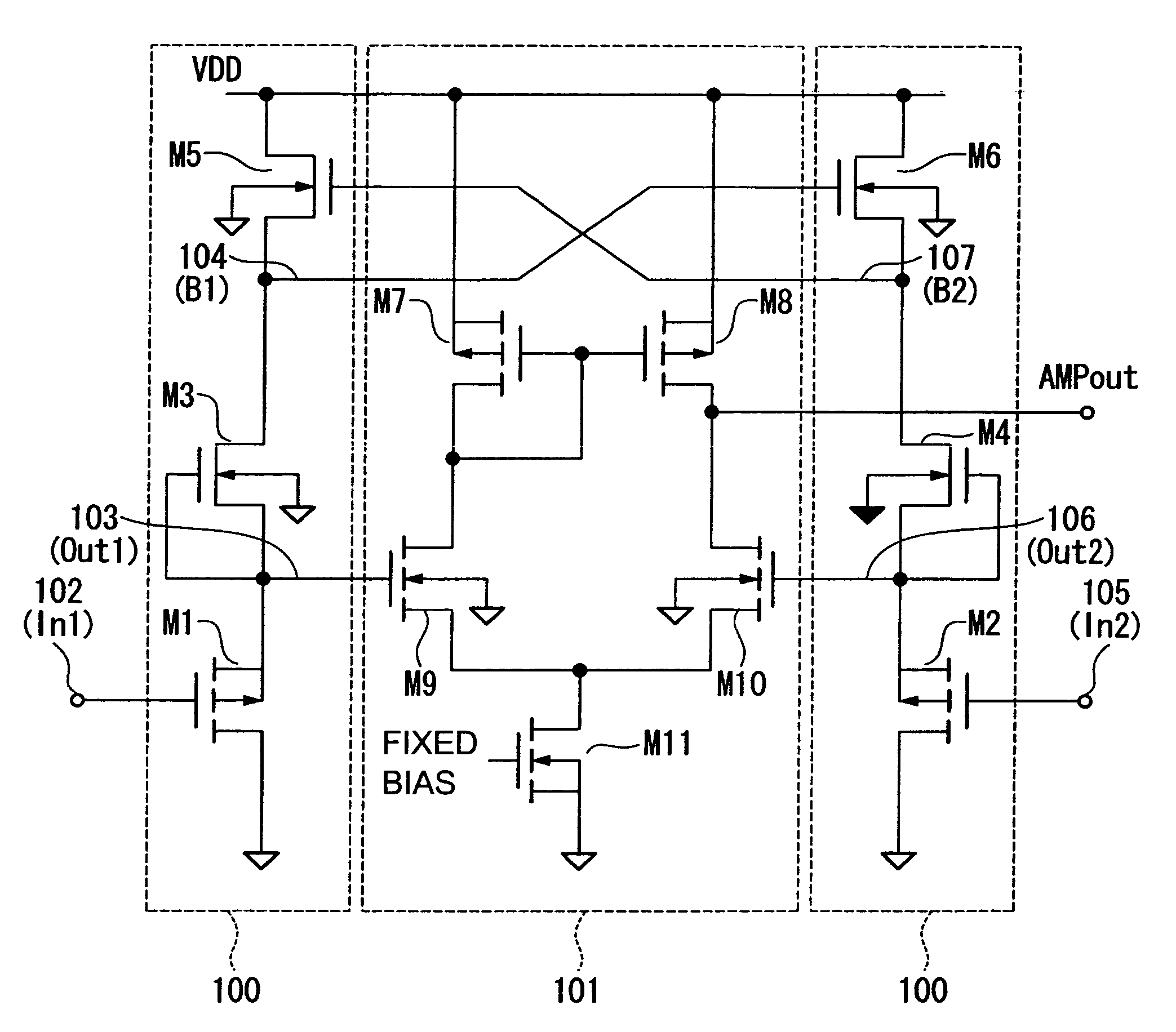
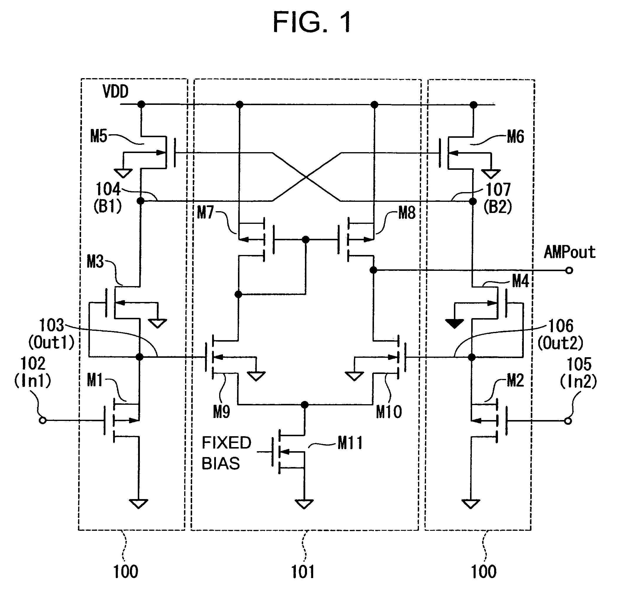
[0047]FIG. 1 illustrates a voltage level shift circuit according to a first embodiment of the present invention. In FIG. 1, portions surrounded by broken lines 100 operate as voltage level shift circuits, while a portion surrounded by a broken line 101 operates as a differential amplifier circuit. Further, the circuits illustrated in FIG. 1 are formed on a P-type substrate.

[0048]A transistor M1 is a P-channel enhancement type MOS transistor, and a first signal input terminal (In1) 102 is connected to its gate. A transistor M3 is an N-channel depletion type MOS transistor, and operates as a constant current source because its gate and its source are connected to each other. In this way, the circuit formed of the transistor M1 and the transistor M3 operates as a source follower circuit with the transistor M3 (constant current source) being a load, and the circuit functions to shift a direct current component of the input voltage of the first signal input terminal (In1) 102 to a positi...

second embodiment

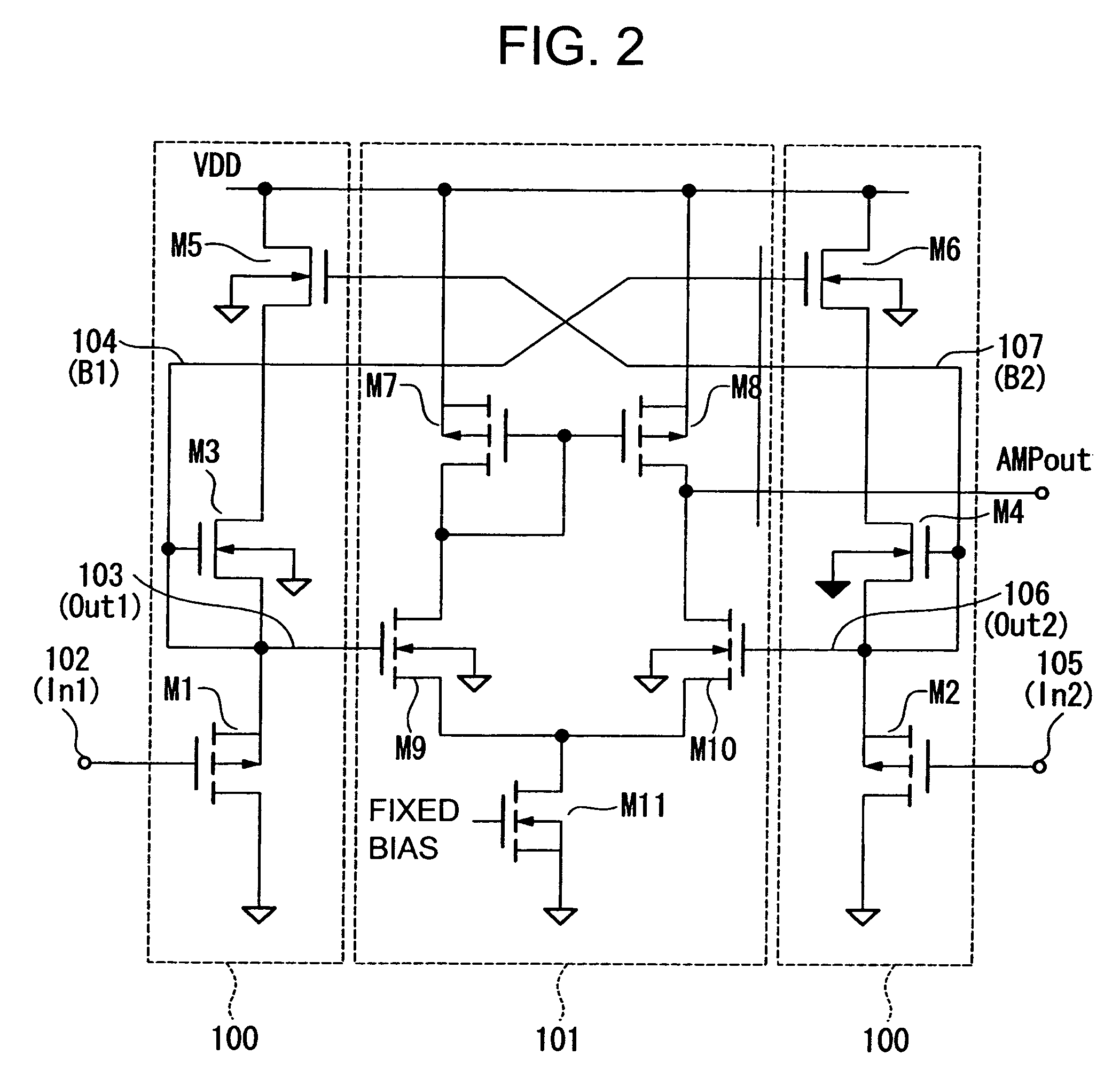
[0064]FIG. 2 illustrates a voltage level shift circuit according to a second embodiment of the present invention.

[0065]In the circuit illustrated in FIG. 2, portions surrounded by broken lines 100 operate as voltage level shift circuits, while a portion surrounded by a broken line 101 operates as a differential amplifier circuit. Further, the circuits illustrated in FIG. 2 are formed on a P-type substrate.

[0066]A P-channel enhancement type MOS transistor M1 operates as a source follower circuit with a constant current source formed of an N-channel depletion type MOS transistor M3 being a load, and functions to shift a direct current component of the input voltage to a positive power supply voltage side and to output the shifted direct current component.

[0067]Therefore, the source follower circuit formed of the transistor M1 and the transistor M3 operates as a first voltage level shift circuit for shifting the direct current component of a signal inputted from the signal input termin...

third embodiment

[0076]FIG. 5 illustrates a voltage level shift circuit according to a third embodiment of the present invention.

[0077]In the voltage level shift circuit illustrated in FIG. 5, a P-channel enhancement type MOS transistor M21 and a P-channel enhancement type MOS transistor M22 form a first voltage level shift circuit (source follower circuit), while a P-channel enhancement type MOS transistor M23 and a P-channel enhancement type MOS transistor M24 form a second voltage level shift circuit (source follower circuit).

[0078]A constant current source 20, a P-channel enhancement type MOS transistor M25, the P-channel enhancement type MOS transistor M22, and the P-channel enhancement type MOS transistor M24 form a current mirror circuit. With this structure, when the constant current source 20 is used to feed constant current (reference current Iref) through the P-channel enhancement type MOS transistor M25, due to the current mirror effect, current I which is the same as the reference curre...


PUM


Abstract

Provided is a voltage level shift circuit including: a first voltage level shift circuit formed of a P-channel enhancement type transistor (M1) and an N-channel depletion type MOS transistor (M3); and a second voltage level shift circuit formed of a P-channel enhancement type transistor (M2) and an N-channel depletion type MOS transistor (M4). In the voltage lever shift circuit, a cascode circuit using an N-channel depletion type transistor (M5) is serially connected to the first voltage level shift circuit, a cascode circuit using an N-channel depletion type transistor (M6) is serially connected to the second voltage level shift circuit, and a unit for complementarily controlling bias voltages of the respective cascode circuits. As a result, an output signal of the voltage level shift circuit connected to an input of a differential amplifier circuit, for expanding an input voltage range of a signal, is not affected by fluctuations in power supply voltage.

Description

[0001]This application claims priority under 35 U.S.C. § 119 to Japanese Patent Application No. JP2006-021764 filed Jan. 31, 2006, the entire content of which is hereby incorporated by reference.BACKGROUND OF THE INVENTION[0002]1. Field of the Invention[0003]The present invention relates to a voltage level shift circuit and a semiconductor integrated circuit including a differential amplifier circuit which uses the voltage level shift circuit. More particularly, the present invention relates to a voltage level shift circuit with improved relative accuracy and improved power supply rejection ratio and to a semiconductor integrated circuit using the voltage level shift circuit.[0004]2. Description of the Related Art[0005]A technique to add a voltage level shift circuit to an input stage of a differential amplifier circuit or the like to expand an input voltage range of the differential amplifier circuit is conventionally widely used (see, for example, JP 05-22054 A).[0006]Such a volta...

Claims


Application Information

Patent Timeline
Patent Type & Authority Patents(United States)
IPC IPC(8): H03L5/00
CPCH03K3/35613H03K3/013G11C5/14
Inventor IMURA, TAKASHI
Owner ABLIC INC
Why Eureka
Try Eureka