Embedded electronic component package

Active Publication Date: 2009-08-11
AMKOR TECH SINGAPORE HLDG PTE LTD
View PDF430 Cites 102 Cited by
  • Summary
  • Abstract
  • Description
  • Claims
  • Application Information

AI Technical Summary

Benefits of technology

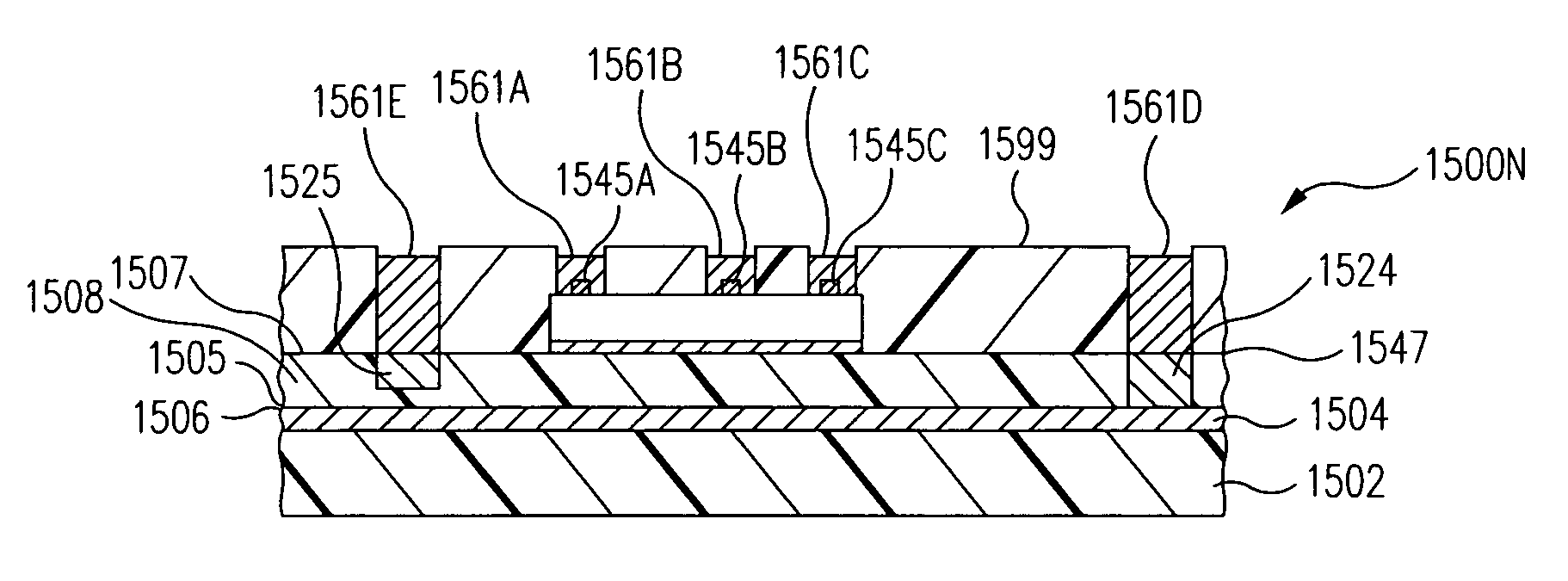
[0017]Thus, in accordance with these embodiments of the present invention, the electronic component is encased in dielectric material. Consequently, the electronic connections to the substrate, and the electronic component itself, are protected and less vulnerable to stress and breakage than prior art systems. In addition, in the one embodiment with the electronic component encased in dielectric material at least partially below the first surface of the first dielectric layer, in accordance with the present invention, surface area is no longer wasted and the resulting device can be made smaller than prior art devices.
[0018]According to this embedded electronic component embodiment of the invention, the bond pads and first electrically conductive vias and traces are directly connected to the corresponding second electrically conductive vias. Stated another way, the bond pads and first electrically conductive vias and traces are electrically connected to th

Problems solved by technology

However, in the wirebond configuration described above, the traces of the substrate were fanned out around the integrated circuit chip, which placed a fundamental restriction on the minimum electronic component package size.
Further, a large impedance was associated with the bond wires.
However, the flip chip bumps between the bond pads of the integrated circuit chip and the traces on the substrate were subject to significant stress, e.g., due to differential thermal expansion between the integrated circuit chip and the substrate.
Thus, failure of the flip chip bumps often occurred which, in turn, decreased yield and increase

Method used


Image

  • Embedded electronic component package
  • Embedded electronic component package
  • Embedded electronic component package

Examples


Example

[0052]Common reference numerals are used throughout the drawings and detailed description to indicate like elements.

DETAILED DESCRIPTION

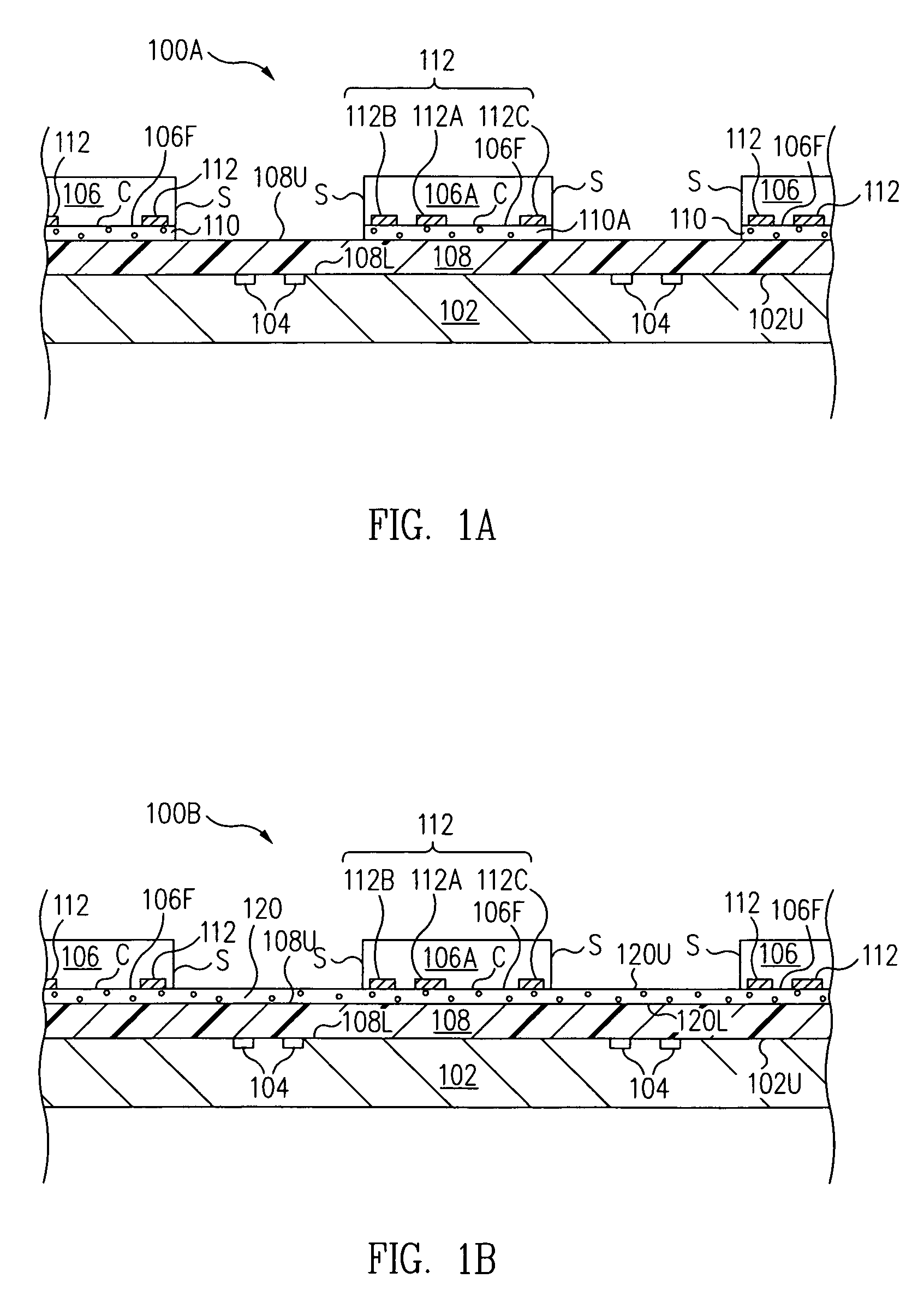
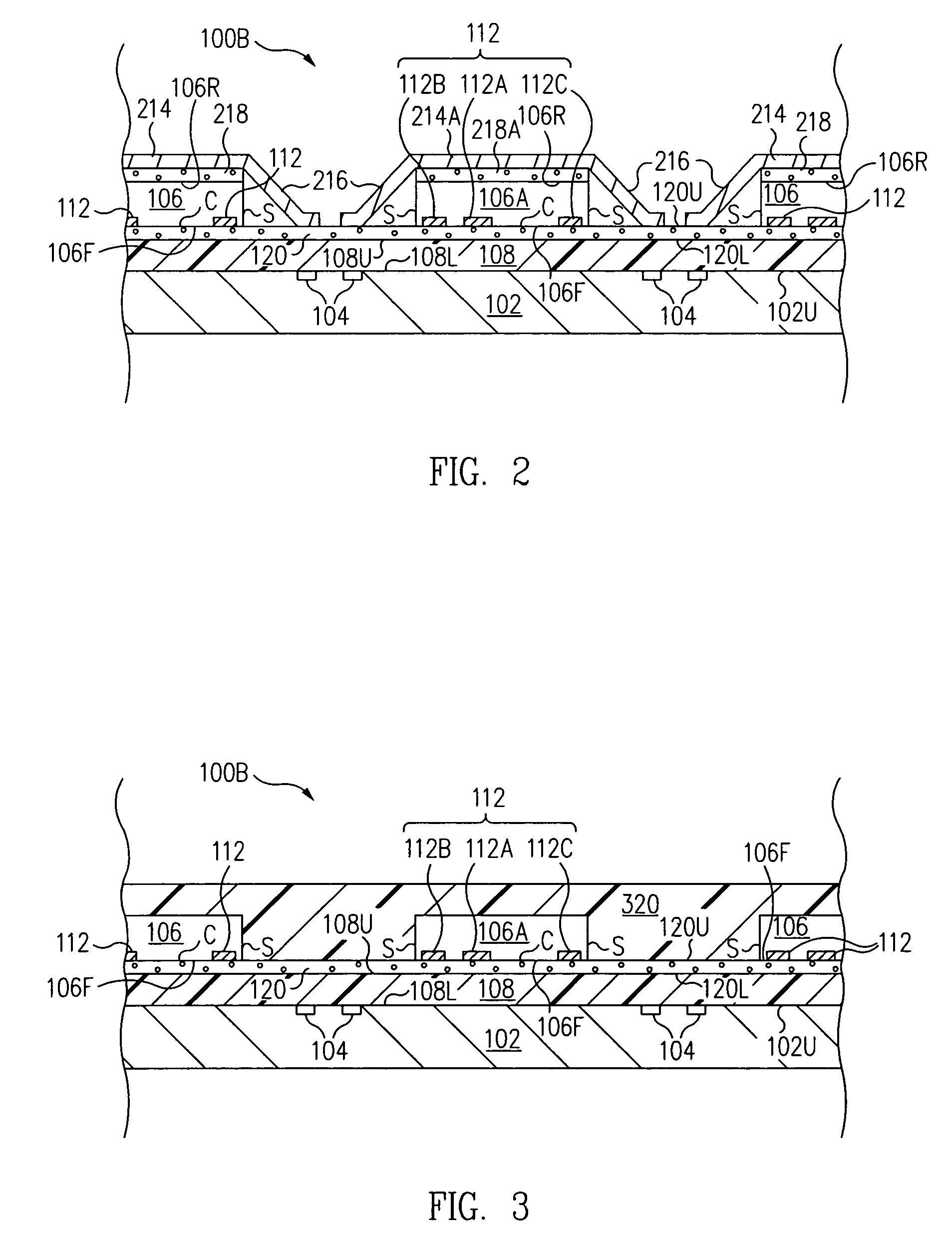
[0053]In accordance with one embodiment of the present invention, a method of forming an electronic component package includes coupling first surfaces 106F of electronic components 106 to a first surface 108U of a dielectric strip 108 with adhesives 110 or 120 (FIGS. 1A and 1B), electronic components 106 having bond pads 112 on first surfaces 106F; forming via apertures 522 through dielectric strip 108 to expose bond pads 112 (FIG. 5); and filling via apertures 522 with an electrically conductive material to form vias 624 electrically coupled to bond pads 112 (FIG. 6).

[0054]Thus, in accordance with this embodiment of the present invention, bond pads 112 are directly connected to corresponding vias 624. Stated another way, bond pads 112 are electrically connected to corresponding vias 624 without the use of a solder, e.g., without the use of flip chi...


PUM


Abstract

A method of forming an embedded electronic component package includes coupling a substrate to a first dielectric layer, strip, or panel, and forming first electrically conductive vias and traces in the first dielectric layer. A cavity is then formed in the first dielectric layer and an electronic component is attached in the cavity. A second dielectric layer, strip, or panel, is then applied to the first dielectric layer, thereby encasing the electronic component in dielectric. Second via apertures are then formed through the second dielectric layer to expose selected electronic component bond pads and/or selected first electrically conductive vias and traces. The second via apertures are then filled with an electrically conductive material to form second electrically conductive vias electrically coupled to selected bond pads and selected first electrically conductive vias and traces.

Description

BACKGROUND OF THE INVENTION[0001]1. Field of the Invention[0002]The present invention relates generally to the packaging of electronic components. More particularly, the present invention relates to an embedded electronic component package and method of fabricating the same.[0003]2. Description of Related Art[0004]One form of an electronic component package included an electronic component such as an integrated circuit chip mounted to a substrate. For example, in a wirebond configuration, the rear surface of the integrated circuit chip was mounted to the substrate, e.g., with an adhesive. Bond wires were used to form the electrical interconnections between the bond pads on the front surface of the integrated circuit chip and the electrically conductive traces on the substrate.[0005]As the art moved to smaller and lighter weight electronic devices, it became increasingly important that the size of the electronic component package used within these electronic devices be as small as po...

Claims


Application Information

Patent Timeline
IPC IPC(8): H01L21/00
CPCH01L21/561H01L23/3128H01L23/5389H01L24/97H01L21/6835H01L24/19H01L2924/15153H01L23/13H01L2221/68345H01L2224/24226H01L2224/24227H01L2224/73267H01L2224/82039H01L2224/82047H01L2224/92144H01L2224/92244H01L2224/97H01L2924/01013H01L2924/01029H01L2924/01047H01L2924/01074H01L2924/01075H01L2924/01078H01L2924/01079H01L2924/01082H01L2924/01322H01L2924/14H01L2924/15311H01L2924/3011H01L2224/12105H01L2224/8203H01L2224/32225H01L2924/014H01L2924/01033H01L2924/01023H01L2924/01006H01L2924/01019H01L2224/82H01L2924/00H01L2224/83005H01L2224/83132H01L2224/05008H01L2224/05026H01L2224/05571H01L2224/05001H01L2224/05139H01L2224/05144H01L2224/05147H01L2224/05155H01L2924/00014H01L2224/04105H01L2224/05599
Inventor HUEMOELLER, RONALD PATRICKRUSLI, SUKIANTOHINER, DAVID J.
Owner AMKOR TECH SINGAPORE HLDG PTE LTD
Why Eureka
Try Eureka