Smart card, smart card module, and a method for production of a smart card module

a smart card module and production method technology, applied in the field of smart cards, can solve the problems of not being able to achieve smart card modules with very small physical heights, unable the active upper surface of the semiconductor chip generally does not offer enough area to produce all the necessary external contacts, etc., to facilitate large-scale production of smart card modules, economic and efficient

Inactive Publication Date: 2009-08-18
INFINEON TECH AG
View PDF11 Cites 22 Cited by
  • Summary
  • Abstract
  • Description
  • Claims
  • Application Information

AI Technical Summary

Benefits of technology

[0009]The present invention replaces conventional smart card modules which have been produced by wire bonding technology by novel smart card modules whose physical height is considerably less than that of such conventional modules. In addition, the present invention facilitates large-scale production of smart card modules in an economic and efficient manner.

Problems solved by technology

The wire bonding method has the major disadvantage that the use of bonding wires restricts to a large degree the miniaturization of the smart card module.
It is not possible to achieve smart card modules with very small physical heights, since the bonding wires have a physical extent which cannot be undershot.
However, one major disadvantage of CSP technology is that the available active upper surface of the semiconductor chip generally does not offer sufficient area to produce all of the necessary external contacts.
Furthermore, CSP technology is unsuitable for the manufacture of smart card modules because the semiconductor chips which are used in smart card modules are subject to significant miniaturization, that is to say to an extremely major “shrink”.
Processing of smart card microcontrollers using CSP technology for production of smart card modules, as proposed in DE 195 00 925 A1, therefore does not appear to be a feasible solution.

Method used


Image

  • Smart card, smart card module, and a method for production of a smart card module
  • Smart card, smart card module, and a method for production of a smart card module
  • Smart card, smart card module, and a method for production of a smart card module

Examples


Embodiment Construction

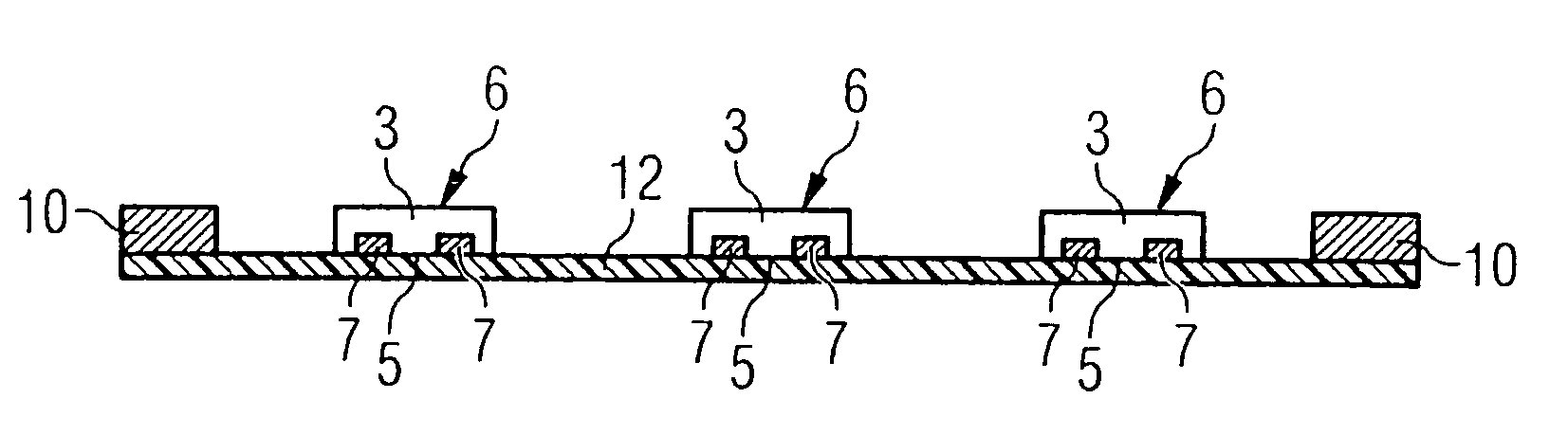
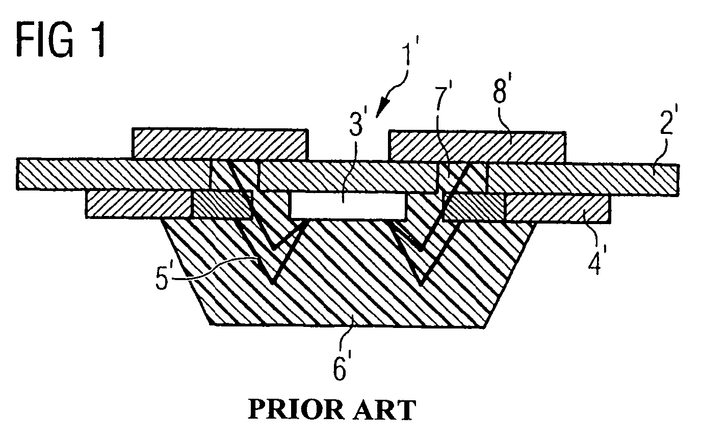
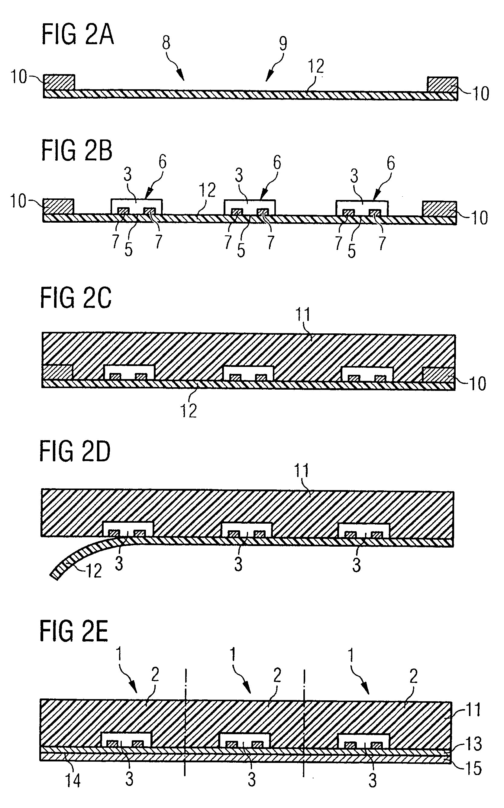
[0014]As noted above, a smart card module is provided in accordance with the present invention that comprises a semiconductor chip including a rear surface, an active upper surface and side surfaces, a plastic housing compound that surrounds the semiconductor chip and includes at least one surface that is coplanar with the active upper surface of the semiconductor chip, and a first dielectric layer arranged on the active upper surface of the semiconductor chip and the at least one surface of the plastic housing compound that is coplanar with the active upper surface of the semiconductor chip. The smart card module further comprises one or more interposer metallization levels that are isolated or separated via further dielectric layers and are connected to the active upper surface of the semiconductor chip, and external contact surfaces that are formed on the outermost interposer level and to which contact metallization is applied for contact data transmission.

[0015]The smart card mo...


PUM


Abstract

A smart card for contact data transmission includes a card body and a smart card module which is fitted in the card body. The smart card module includes a semiconductor chip with an active upper surface, a plastic housing compound that surrounds the semiconductor chip and includes at least one surface that is coplanar with the active upper surface of the semiconductor chip, a first dielectric layer that is arranged on the plastic housing compound surface and on the active upper surface of the semiconductor chip, one or more interposer metallization levels, which are isolated via further dielectric layers and are connected to the active upper surface of the semiconductor chip, and external contact surfaces. The external contact surfaces are formed on the outermost interposer level and facilitate contact data transmission. The smart card module uses no bonding wires and has a very small physical volume.

Description

CROSS REFERENCE TO RELATED APPLICATIONS[0001]This application is a continuation of PCT / DE2004 / 001363, filed Jun. 28, 2004, and titled “Smart Card, Smart Card Module, and a Method for Production of a Smart Card Module,” which claims priority under 35 U.S.C. §119 to German Application No. 103 34 578.7, filed on Jul. 28, 2003, and titled “Smart Card, Smart Card Module, and a Method for Production of a Smart Card Module,” the entire contents of which are hereby incorporated by reference.FIELD OF THE INVENTION[0002]The invention relates to a smart card for contact data transmission, including a card body and a smart card module which is fitted in the card body. The invention also relates to a smart card module and to a method for production of a smart card module.BACKGROUND[0003]Smart cards and smart card modules have been known for a long time. For example, in DE 195 00 925 A1, a smart card module is described including a substrate on which a semiconductor chip and metallic connecting p...

Claims


Application Information

Patent Timeline
Patent Type & Authority Patents(United States)
IPC IPC(8): G06K19/00G06K19/077H01L21/56H01L21/60H01L21/68H01L23/31H01L23/498H01L23/538
CPCG06K19/07743G06K19/07747H01L21/561H01L21/566H01L21/568H01L23/3107H01L23/49855H01L23/5389H01L24/96G06K19/07745H01L2224/48227H01L2224/48228H01L2224/48247H01L2224/49109H01L2924/01032H01L2924/01075H01L2924/01068H01L2924/01033H01L24/48H01L24/49H01L2924/01005H01L2924/01006H01L2924/00H01L2924/00014H01L2924/181H01L2924/00012H01L2224/45099H01L2224/45015H01L2924/207
Inventor FUERGUT, EDWARDGOLLER, BERNDHAGEN, ROBERT-CHRISTIANJEREBIC, SIMONPOHL, JENSSTROBEL, PETERWOERNER, HOLGER
Owner INFINEON TECH AG
Why Eureka
Try Eureka