Semiconductor device having a high withstand voltage

a technology of high withstand voltage and semiconductors, which is applied in the direction of semiconductor devices, basic electric elements, electrical appliances, etc., can solve the problems of limited current escape routes and achieve the effects of small damage by heat generation, less current concentration in the end portion of the conducting portion, and not large width

Inactive Publication Date: 2009-08-25
TOYOTA JIDOSHA KK
View PDF13 Cites 1 Cited by
  • Summary
  • Abstract
  • Description
  • Claims
  • Application Information

AI Technical Summary

Benefits of technology

[0013]In this semiconductor device, when the active device is switched off, residual carriers in the active device escape to the contact electrode. This current escaping route is limited to the conducting portion of the active device and the contact electrode. Herein, since the marginal corner of the conducting portion is formed with a curved line or with an obtuse angle, the current of the conducting portion into the corner is dispersed somewhat. Hence, current density is not excessively high at the apex of edge. Hence, damage by heat generation is small. On the other hand, the ON voltage is not particularly high. This is because area of the conducting portion is not increased. Hence, carriers do not pass too much into the contact electrode in ON state.
[0015]Further, the semiconductor device of the invention may have, instead of the feature (1) or (2), a feature (3) that impurity concentration is lower at an end portion of conducting portion of the active device and the contact electrode than in the central portion of it. As a result, current concentration at the end portion of conducting portion is lessened. This is because the end portion with lower impurity concentration has a higher resistance, so that current is more likely to flow into the central portion with lower resistance. On the other hand, area is not increased in the entire conducting portion. To the contrary, since the end portion has a higher resistance, the entire conducting portion has a slightly increased resistance. Therefore, local heat generation after switching off is prevented, while the ON voltage in ON state is low.

Problems solved by technology

This current escaping route is limited to the conducting portion of the active device and the contact electrode.
Hence, damage by heat generation is small.

Method used


Image

  • Semiconductor device having a high withstand voltage
  • Semiconductor device having a high withstand voltage
  • Semiconductor device having a high withstand voltage

Examples


first embodiment

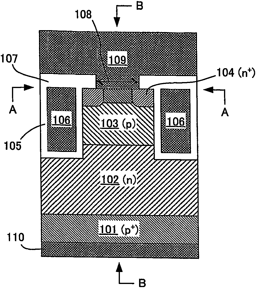
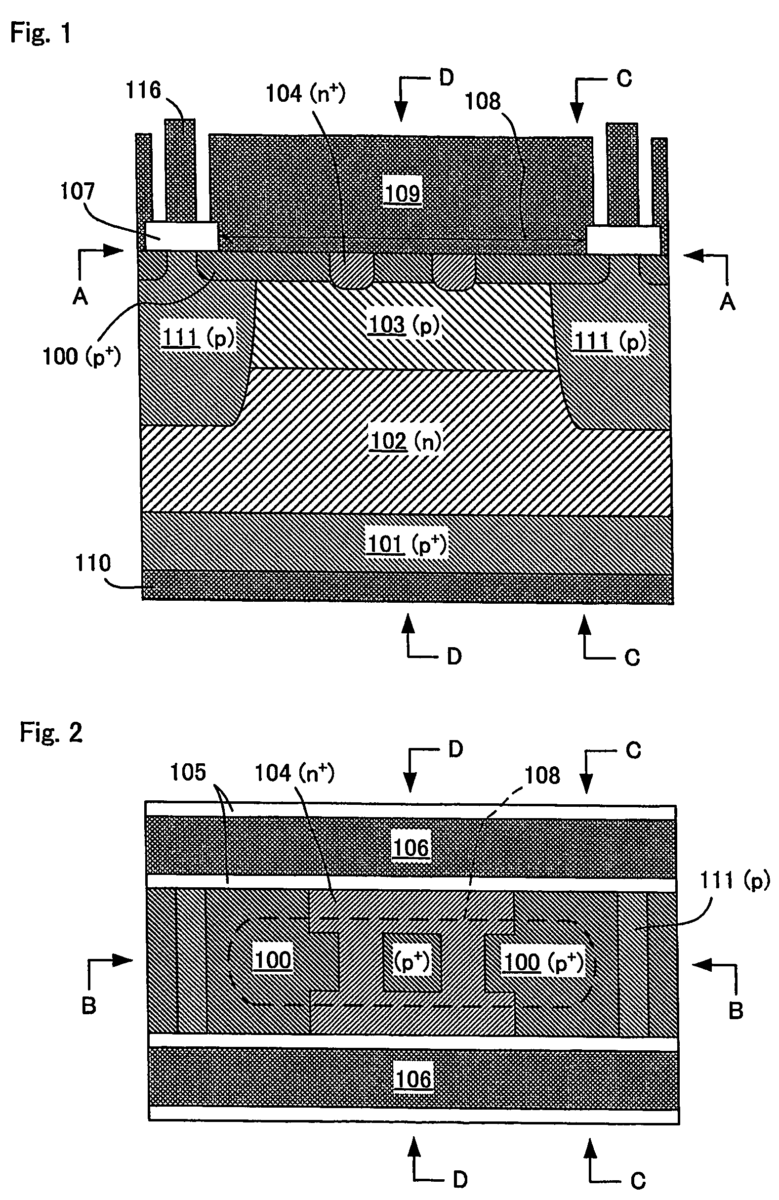
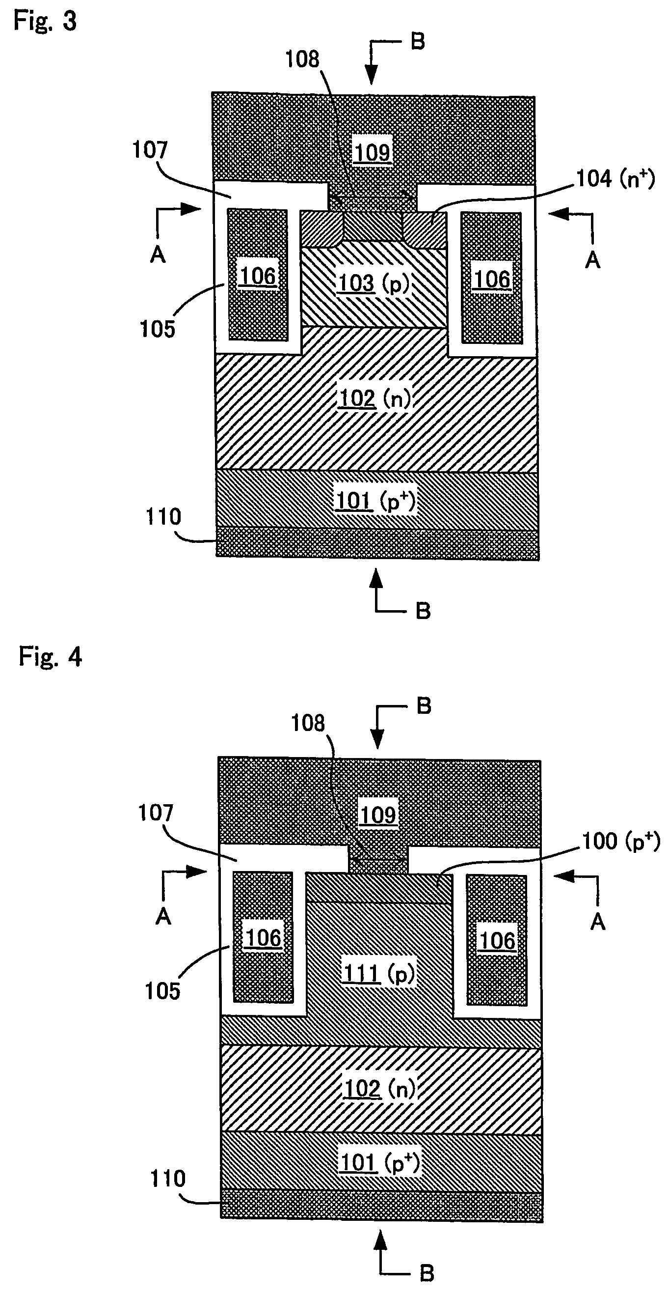
[0042]A structure of an insulated gate field-effect semiconductor device according to a first embodiment is described by referring to FIG. 1 to FIG. 4. FIG. 1, FIG. 3, and FIG. 4 are longitudinal sectional views, and FIG. 2 is a plan sectional view at level A-A in these drawings. FIG. 1 is a sectional view of position B-B in FIG. 2 to FIG. 4. FIG. 3 is a sectional view of position D-D in FIG. 1 and FIG. 2. FIG. 4 is a sectional view of position C-C in FIG. 1 and FIG. 3.

[0043]In the insulated gate semiconductor device shown in FIG. 1 to FIG. 4, on the principal plane of level A-A side of semiconductor substrate, N+ emitter region 104 of high impurity concentration and P+ emitter region 100 of high impurity concentration are provided. Contacting with the lower part of them, P body region 103 is disposed. Further beneath the P body region 103, N drift region 102 is provided, and P+ collector region 101 is provided furthermore beneath. So far is within a semiconductor substrate. In the ...

second embodiment

[0058]A structure of an insulated gate field-effect semiconductor device according to a second embodiment is described by referring to FIG. 13 and FIG. 14. FIG. 13 is a longitudinal sectional view, and a plane sectional view at level A-A thereof is FIG. 14. FIG. 13 is a sectional view of position C-C in FIG. 14. A sectional view of position B-B in FIG. 13 and FIG. 14 is same as FIG. 1 relating to the first embodiment except that the reference numerals 1** are changed to 2**. A sectional view of position D-D in FIG. 14 is same as FIG. 3 relating to the first embodiment except that the reference numerals are changed similarly. In the following explanation of the embodiment, when referring to FIG. 1 and FIG. 3, it is supposed that the reference numerals are changed in such manner.

[0059]In the insulated gate field-effect semiconductor device of the embodiment, what differs from the insulated gate field-effect semiconductor device of the first embodiment lies only in the plane shape of t...

third embodiment

[0064]A structure of an insulated gate field-effect semiconductor device according to a third embodiment is described by referring to FIG. 16 and FIG. 17. FIG. 16 is a plane sectional view, and a longitudinal sectional view at position C-C thereof is FIG. 17. FIG. 16 is a sectional view of level A-A in FIG. 17. A sectional view of position B-B in FIG. 16 and FIG. 17 is same as FIG. 1 relating to the first embodiment except that the reference numerals 1** are changed to 3**. A sectional view of position D-D in FIG. 16 is same as FIG. 3 relating to the first embodiment except that the reference numerals are changed similarly. In the following explanation of the embodiment, when referring to FIG. 1 and FIG. 3, it is supposed that the reference numerals are changed in such manner.

[0065]In the insulated gate field-effect semiconductor device of the embodiment, what differs from the insulated gate field-effect semiconductor device of the first embodiment lies only in the impurity concentr...


PUM


Abstract

To present a semiconductor device capable of operating stably even at large current, by lessening current concentration into the corners of contact opening after switching off and suppressing local heat generation without raising the ON voltage. In an insulated gate transistor divided by P field region 111 and gate electrode 106, having N+ emitter region 104 and P+ emitter region 100, and controlling conduction between emitter and collector by voltage applied to gate electrode 106, the shape of contact opening 108 contacting emitter (N+ emitter region 104 and P+ emitter region 100) and emitter electrode is formed of curved lines at four corners. Hence, eliminating right-angle apex, hole current from the field region into the emitter electrode after switching off is prevented from concentrating at one point.

Description

[0001]This is a 371 national phase application of PCT / JP2004 / 008516 filed 10 Jun. 2004, claiming priority to Japanese Patent Application No. 2003-195498 filed 11 Jul. 2003, the contents of which are incorporated herein by reference.TECHNICAL FIELD[0002]The present invention relates to a semiconductor device of high withstand voltage suited to switching of large current. More particularly, it relates to a semiconductor device intended to prevent overheating when switching off.BACKGROUND ART[0003]As conventional semiconductor devices, insulated gate semiconductor devices disclosed in patent references 1 and 2 are known. In these insulated gate semiconductor devices, by applying a gate voltage to an insulated gate, a field effect is produced in a channel region in a semiconductor substrate, and current flows between emitter and collector. Accordingly, a contact opening is provided in order to exchange carriers between an emitter region and an emitter electrode. A typical example of thi...

Claims


Application Information

Patent Timeline
Patent Type & Authority Patents(United States)
IPC IPC(8): H01L29/76H01L29/94H01L31/062H01L31/113H01L31/119H01L21/28H01L29/06H01L29/417H01L29/423H01L29/739H01L29/78
CPCH01L29/0696H01L29/42324H01L29/41741
Inventor NISHIWAKI, KATSUHIKO
Owner TOYOTA JIDOSHA KK
Why Eureka
Try Eureka