MEMS switches having non-metallic crossbeams

a technology of non-metallic crossbeams and switches, applied in the field of microelectromechanical system switches, can solve the problems of low cost, complicated integration with other ics, and high cost of fabrication, and achieve the effects of low cost, simple structure, and simple structur

Inactive Publication Date: 2009-09-01
NASA
View PDF16 Cites 22 Cited by
  • Summary
  • Abstract
  • Description
  • Claims
  • Application Information

AI Technical Summary

Benefits of technology

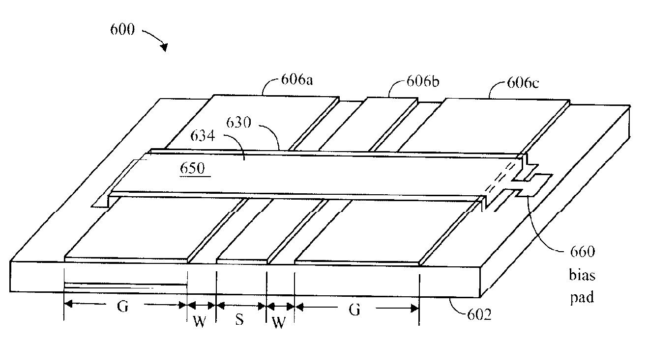
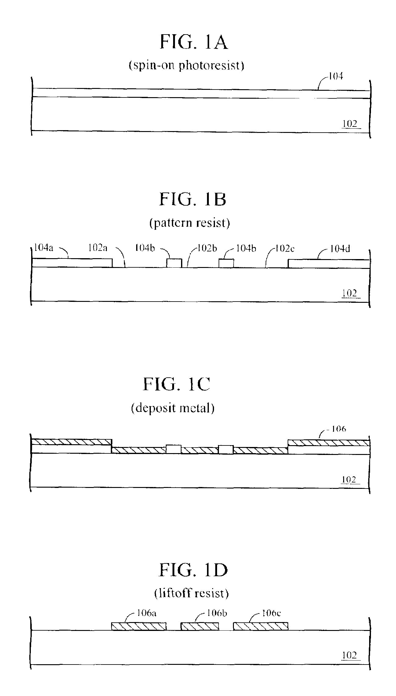
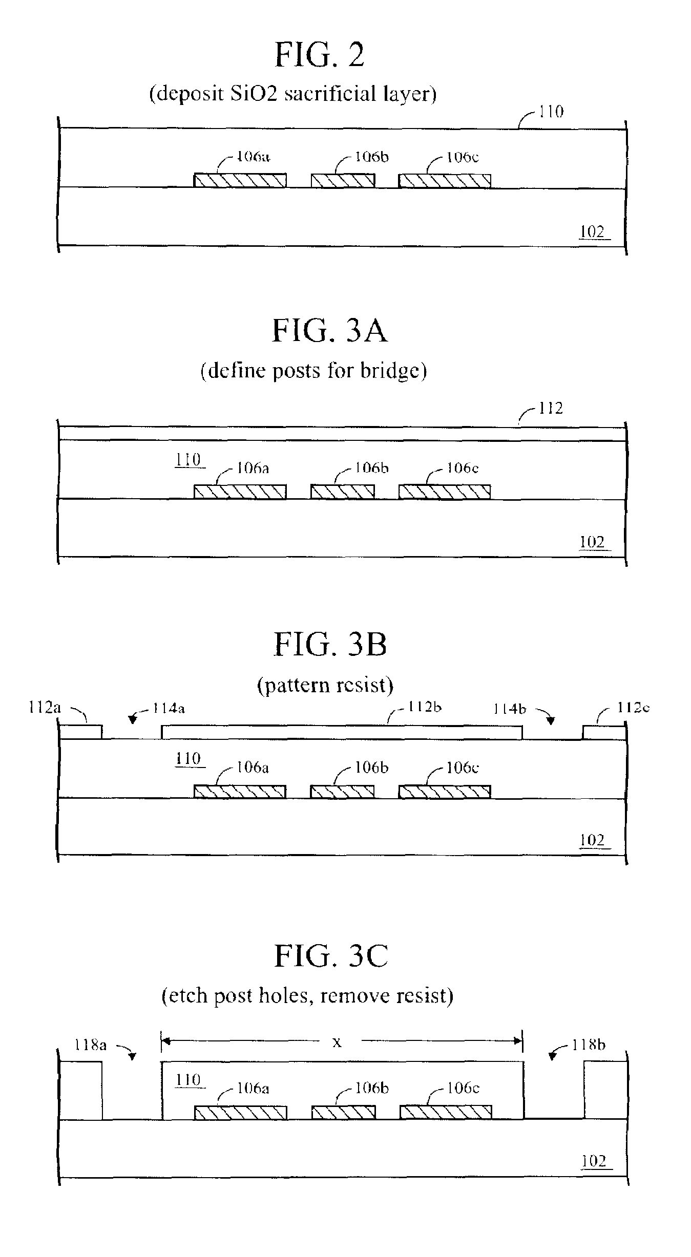
[0076]The switch may be fabricated with conventional silicon (Si) integrated circuit (IC) processing techniques, which makes it a low cost device. The design of the switch is very versatile and can be implemented in many transmission line (TL) mediums.
[0077]The non-metallic thin film bridge / cantilevers may comprise silicon carbide (SiC), which demonstrates controlled stress and conductivity. SiC is most widely known as a structural material for MEMS devices designed to operate in harsh environments, such as high temperature, radiation, wear, etc. However, SiC is also attractive in RF MEMS applications, due to its high Young Modulus-to-density ratio. When used as the structural material in micromachined bridges / cantilevers, the inherent stiffness and tensile stresses of SiC will result in beams that are completely resistant to sagging and failure. This property makes SiC an ideal alternative to metals in bridge-based RF MEMS switches, which currently suffer from severe sagging and failure during operation. Moreover, SiC is highly resistant to oxidation which, when coupled with its overall chemical resistance, makes SiC surfaces virtually stiction-free, a significant advantage when the material is to be fabricated into narrow gapped, micromachined bridges for use as contact switches.
[0078]A thin metal layer is placed over the SiC bridge, for biasing the device. The supporting layer of SiC would physically contact the center conductor. Use of SiC for the bridge / cantilever would forestall metal fatigue, and enables a low-voltage DC bias for actuation, while enabling well-known and economical CMOS manufacturing methods. SiC is also very hard and strong, chemically inert, and resistant to stiction. (Applying appropriate voltages causes an attractive force deforming the elongate beam of the cantilever / bridge.)
[0079]Incorporation of non-metallic thin films such as SiC as the main mechanical structure in bridge-based RF switches eliminates the need to use a stiction-preventing insulating film between the bridge and transmission line, because the SiC itself is highly resistant to stiction, due to its chemical inertness coupled with its resistance to oxidation. As a result only a low voltage DC bias is needed to actuate the SiC MEMS device, whereas all capacitive MEMS switches (MEMS devices which require an insulator to prevent stiction) require a low frequency peak-to-peak voltage waveform to prevent charge trapping which seriously degrades the performance of the switch and complicates the biasing structure of the overall system. In use, the beam of the bridge / cantilever deflects (when biased) and touches the transmission lines, shorting them out.
[0080]Due to the physical properties of the non-metal SiC film, the switch can withstand and operate in harsh environments as well as survive high power applications. This may include wireless sensor applications for aircraft or rocket engines as well as for internal switching application within the engines themselves. Also, the RF MEMS switch device disclosed herein has the potential to be the first extremely low loss MEMS device that can be space qualified.
[0081]The RF MEMS switch disclosed herein utilizes bridges / cantilevers constructed from Silicon Carbide (SiC). In general, these switches consist of a single or double supported cantilever suspended over a microwave transmission line. In its “up” state, the cantilever is several microns above the transmission line and does not affect the electromagnetic fields flowing through the transmission lines. When the actuation voltage is applied between the cantilever and transmission lines, the cantilever is pulled “down” and makes contact with the circuit just as with a typical MEMS switch. The SiC film is non metallic so there is no welding problem which occurs with the metal-to-metal type MEMS switches after prolonged use, and therefore the reliability of the life time of the switch is dramatically increased. Furthermore, because SiC is conductive, due to ion implantation, and takes the place of the insulating film found in capacitive MEMS switches, the switch requires only a DC actuation voltage to operate.

Problems solved by technology

They can be very lossy, expensive to fabricate, and complicate integration with other ICs.
However, MEMS switches are generally much slower than solid-state switches.
This speed limitation precludes applying MEMS switches in certain technologies, such as wireless communications, where sub-microsecond switching is required.
This type of switch requires a DC voltage to actuate but suffers from the metal contacts wearing down and welding after prolonged use, thus causing the switch to fail.
The low frequency peak-to-peak voltage waveform is needed to prevent charge trapping within the insulator film and seriously degrades the performance of the switch and complicates the biasing structure of the overall system.
However, the greatest disadvantage of the two types (contact and capacitive) of MEMS switches is that they utilize metal bridge / cantilever structures that are very unreliable due to severe sagging and eventual failure during prolonged operations.
This drastically reduces the reliability of the switches.
Reliability is the single most important issue now prohibiting metal-based RF MEMS switches from being implemented in a wide range of commercial applications, as well as applications for military and space.
In addition, the actuation voltage may deflect the cantilever away from the conductive pad.
In particular, even when the beam or the contact unit under the beam is unbalanced, the contact unit can elastically contact the beam to obtain a stable electrical switching operation.
The ions introduce both a chemical change in the target, in that they can be a different element than the target, and a structural change, in that the crystal structure of the target can be damaged or even destroyed.

Method used


Image

  • MEMS switches having non-metallic crossbeams
  • MEMS switches having non-metallic crossbeams
  • MEMS switches having non-metallic crossbeams

Examples


Embodiment Construction

[0099]Throughout the descriptions set forth herein, lowercase numbers or letters may be used, instead of subscripts. For example Vg could be written Vg. Generally, lowercase is preferred to maintain uniform font size.) Regarding the use of subscripts (in the drawings, as well as throughout the text of this document), sometimes a character (letter or numeral) is written as a subscript—smaller, and lower than the character (typically a letter) preceding it, such as “Vs” (source voltage) or “H2O” (water). For consistency of font size, such acronyms may be written in regular font, without subscripting, using uppercase and lowercase—for example “Vs” and “H2O”.

[0100]Although various features of the invention may be described in the context of a single embodiment, the features may also be provided separately or in any suitable combination. Conversely, although the invention may be described herein in the context of separate embodiments for clarity, the invention may also be implemented in ...


PUM


Abstract

A RF MEMS switch comprising a crossbeam of SiC, supported by at least one leg above a substrate and above a plurality of transmission lines forming a CPW. Bias is provided by at least one layer of metal disposed on a top surface of the SiC crossbeam, such as a layer of chromium followed by a layer of gold, and extending beyond the switch to a biasing pad on the substrate. The switch utilizes stress and conductivity-controlled non-metallic thin cantilevers or bridges, thereby improving the RF characteristics and operational reliability of the switch. The switch can be fabricated with conventional silicon integrated circuit (IC) processing techniques. The design of the switch is very versatile and can be implemented in many transmission line mediums.

Description

STATEMENT REGARDING FEDERALLY SPONSORED RESEARCH OR DEVELOPMENT[0001]The invention described herein was made by an employee of the United States Government and may be manufactured and used by or for the Government for Government purposes without the payment of any royalties thereon or therefore.TECHNICAL FIELD[0002]The invention relates to microelectromechanical system (MEMS) switches and, more particularly, to MEMS switches for radio frequency (RF) and microwave applications.BACKGROUND[0003]Currently in RF applications there are two types of switches that can be used to perform switching functions. The most popular and commercially available is the semiconductor device. This includes such devices as PIN diodes, field effect transistors (FETs) and heterojunction bipolar transistors (HBTs). They can be very lossy, expensive to fabricate, and complicate integration with other ICs. The other switch, more recently developed and commercially available to a limited extent, is the RF MEMS ...

Claims


Application Information

Patent Timeline
Patent Type & Authority Patents(United States)
IPC IPC(8): H01P1/10H01P5/00
CPCH01P1/127
Inventor SCARDELLETTI, MAXIMILLIAN C
Owner NASA
Why Eureka
Try Eureka