Semiconductor memory and refresh cycle control method

a technology of memory and memory cells, applied in the direction of information storage, static storage, digital storage, etc., can solve the problems of data loss, short refresh cycle, etc., and achieve the effect of reducing standby curren

Inactive Publication Date: 2009-09-01
SOCIONEXT INC
View PDF11 Cites 42 Cited by
  • Summary
  • Abstract
  • Description
  • Claims
  • Application Information

AI Technical Summary

Benefits of technology

[0021]The present invention was made under the background circumstances described above. An object of the present invention is to provide a semiconductor memory that can reduce a standby current by properly changing a refresh cycle according to the temperature of the semiconductor memory.
[0022]Another object of the present invention is to provide a refresh cycle control method that can reduce a standby current by properly changing a refresh cycle according to temperature.

Problems solved by technology

Usually a refresh cycle becomes short if an electric current outputted from a constant current generation circuit is large.
In addition, the following problem arises because a refresh cycle extension rate is uniform.
If the refresh cycle exceeds the data retention time, data held in a memory cell is lost.

Method used


Image

  • Semiconductor memory and refresh cycle control method
  • Semiconductor memory and refresh cycle control method
  • Semiconductor memory and refresh cycle control method

Examples


first embodiment

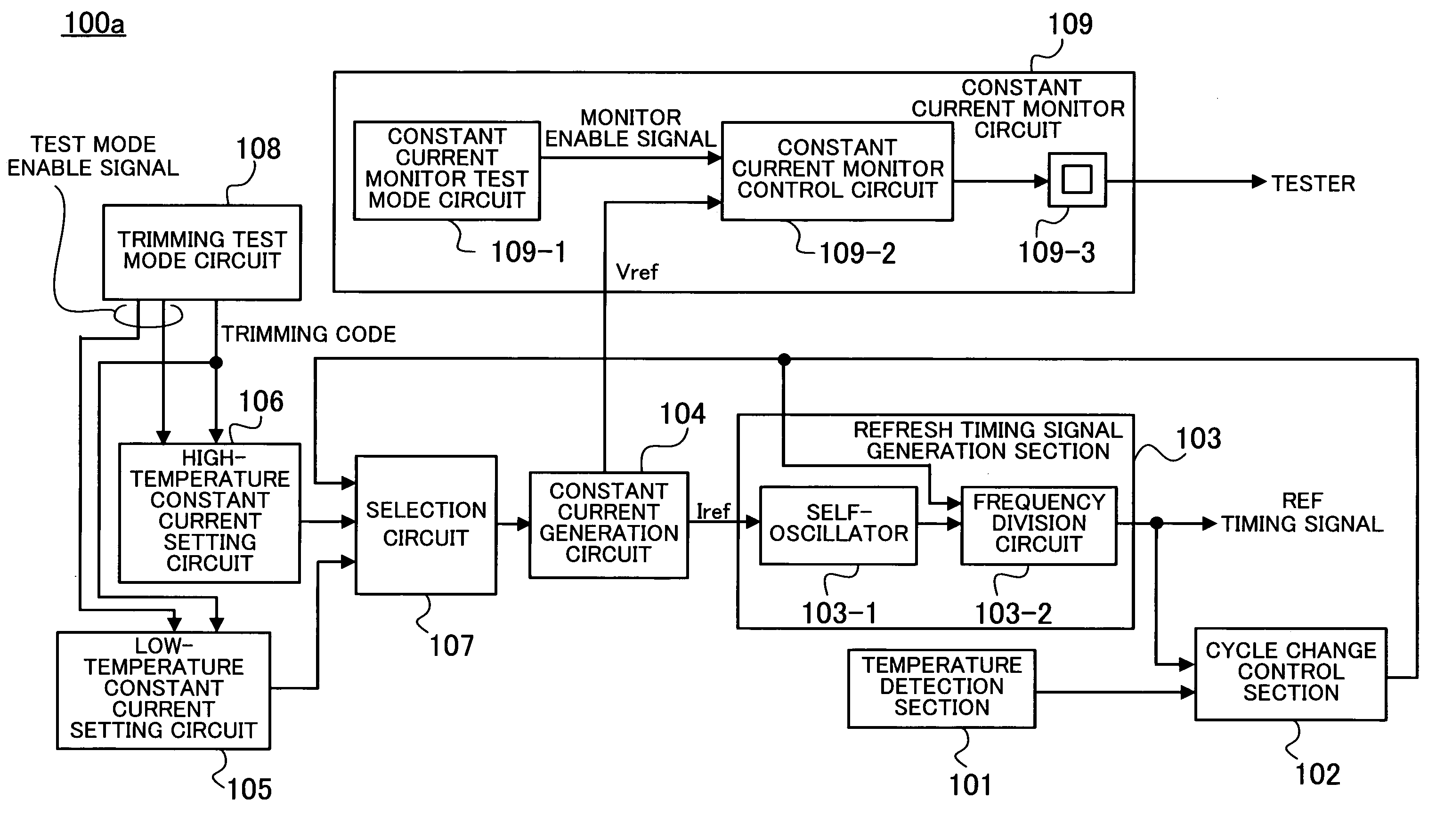
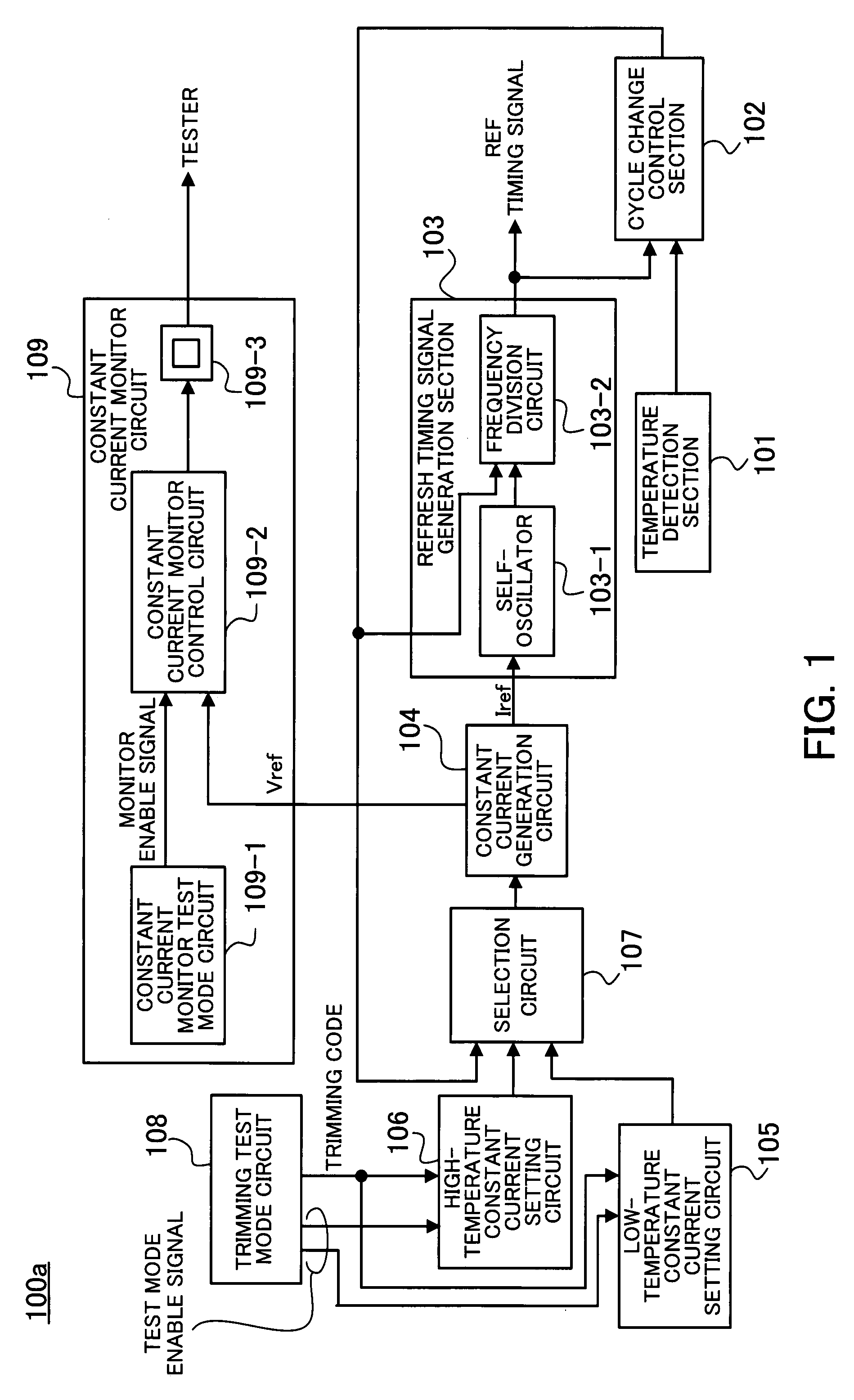
[0037]FIG. 1 shows the structure of a semiconductor memory according to the present invention.

[0038]A semiconductor memory 100a according to a first embodiment of the present invention comprises a temperature detection section 101 for detecting temperature, a cycle change control section 102, a refresh timing signal generation section 103, a constant current generation circuit 104, a low-temperature constant current setting circuit 105, a high-temperature constant current setting circuit 106, a selection circuit 107, a trimming test mode circuit 108, and a constant current monitor circuit 109.

[0039]The temperature detection section 101 detects the temperature of the semiconductor memory 100a.

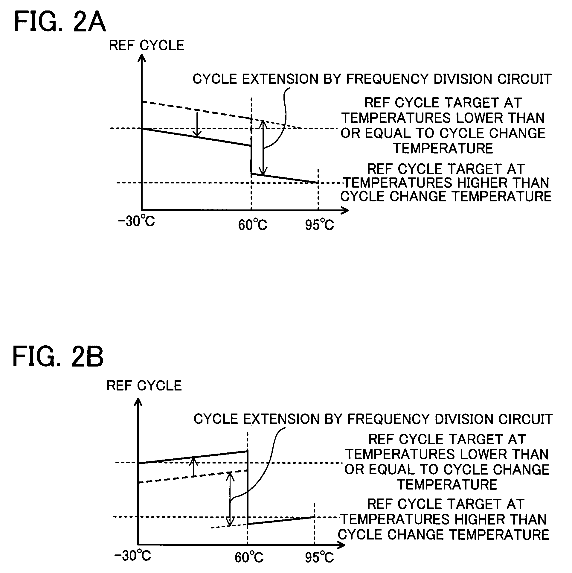
[0040]When temperature detected by the temperature detection section 101 reaches a cycle change temperature (60° C., for example), the cycle change control section 102 sends a cycle change signal for changing a refresh cycle.

[0041]The refresh timing signal generation section 103 includes a self-...

second embodiment

[0077]A semiconductor memory according to the present invention will now be described.

[0078]FIG. 6 shows the structure of a semiconductor memory according to a second embodiment of the present invention.

[0079]Components of a semiconductor memory according to a second embodiment of the present invention that are the same as those of the semiconductor memory 100a according to the first embodiment of the present invention are marked with the same symbols and descriptions of them will be omitted.

[0080]A semiconductor memory 100b according to a second embodiment of the present invention differs from the semiconductor memory 100a according to the first embodiment of the present invention in that it includes a temperature dependence information storage section 130 for storing information indicative of the dependence of current Iref on temperature measured at test time. In addition, a selection circuit 107a included in the semiconductor memory 100b differs partly from the selection circuit ...

third embodiment

[0084]A semiconductor memory according to the present invention will now be described.

[0085]FIG. 7 shows the structure of a semiconductor memory according to a third embodiment of the present invention.

[0086]Components of a semiconductor memory according to a third embodiment of the present invention that are the same as those of the semiconductor memories 100a and 100b according to the first embodiment and the second embodiment, respectively, of the present invention are marked with the same symbols and descriptions of them will be omitted.

[0087]As with the semiconductor memory 100b according to the second embodiment of the present invention, a semiconductor memory 100c according to a third embodiment of the present invention includes a temperature dependence information storage section 130 for storing the dependence of current Iref on temperature. Unlike the semiconductor memory 100b according to the second embodiment of the present invention, however, the semiconductor memory 100...


PUM


Abstract

A semiconductor memory and a refresh cycle control method that reduce a standby current by properly changing a refresh cycle according to the temperature of the semiconductor memory. A temperature detection section detects the temperature of the semiconductor memory. A cycle change control section sends a cycle change signal for changing a refresh cycle when the temperature of the semiconductor memory reaches a predetermined cycle change temperature. A refresh timing signal generation section generates a refresh timing signal and changes the cycle of the refresh timing signal in response to the cycle change signal. A constant current generation circuit generates an electric current for generating the refresh timing signal. A low-temperature constant current setting circuit designates the level of the electric current generated in the case that the temperature of the semiconductor memory is lower than or equal to the cycle change temperature. A high-temperature constant current setting circuit designates the level of the electric current generated in the case that the temperature of the semiconductor memory is higher than the cycle change temperature.

Description

CROSS-REFERENCE TO RELATED APPLICATIONS[0001]This application is based upon and claims the benefits of priority from the prior Japanese Patent Application No. 2006-140605, filed on May 19, 2006, the entire contents of which are incorporated herein by reference.BACKGROUND OF THE INVENTION[0002](1) Field of the Invention[0003]This invention relates to a semiconductor memory and a refresh cycle control method, and more particularly to a semiconductor memory, such as a dynamic random access memory (DRAM), which needs refresh operation and a refresh cycle control method.[0004](2) Description of the Related Art[0005]A technique for making the oscillation cycle of a self-oscillator on the basis of which the refresh cycle of a DRAM is determined constant by using an electric current generated by a constant current generation circuit is known.[0006]In a process of testing a device, a predetermined number of fuses from a plurality of fuses used in a circuit included in a semiconductor memory ...

Claims


Application Information

Patent Timeline
Patent Type & Authority Patents(United States)
IPC IPC(8): G11C7/00
CPCG11C7/04G11C11/401G11C11/406G11C11/40626G11C29/02G11C29/028G11C2029/0409G11C2029/5002G11C2211/4061G11C2211/4067G11C11/4076
Inventor MORI, KAORU
Owner SOCIONEXT INC
Why Eureka
Try Eureka