Method for manufacturing patterned porous molded product or nonwoven fabric, and electric circuit component

a technology of porous molded products and nonwoven fabrics, applied in the direction of porous dielectrics, synthetic resin layered products, woven fabrics, etc., can solve the problems of unfavorable formation of flashes upon blanking, difficult to apply methods according, and difficulty in fine processing, etc., to achieve low cost, less damage, and easy to cut

Inactive Publication Date: 2009-09-08
SUMITOMO ELECTRIC IND LTD
View PDF26 Cites 9 Cited by
  • Summary
  • Abstract
  • Description
  • Claims
  • Application Information

AI Technical Summary

Benefits of technology

[0025]In accordance with a method of the present invention, the fine and complicated pattern formation onto a soft porous material which has been very difficult with conventional mechanical processing is possible. With the method of the invention, it is possible to carry out fluid processing such as sand blasting onto a porous material under the conditions causing less damages to a mask. This allows the-formation of fine trenches and through holes with simplicity. Namely, in accordance with the invention, deep trench processing and through hole processing are possible in a porous molded product or a nonwoven fabric which is too soft and very difficult to cut, and also, the porous structure will not be broken. The method of the invention achieves low cost and is suitable for mass production.
[0026]Further, in accordance with the invention, an electric circuit component such as a soft and low relative dielectric constant circuit substrate is provided. With the electric circuit component of the invention, the stress concentration due to load distortion or heat distortion is less likely to occur at an interface between a substrate and a circuit. With the electric circuit component of the invention, a porous material absorbs distortion, and hence overload is less likely to occur in wiring, and disconnection is less likely to occur.

Problems solved by technology

However, with such mechanical processing methods, fine processing may be difficult, or the methods are difficult to apply according to the material of the substrate.
However, the formation of flash upon blanking has been unfavorably inevitable.
Therefore, fine processing is difficult, and in addition, the method is not suitable for processing trenches having a wide variety of patterns.
However, with a conventional sand blast processing, the formation of fine-pitch wiring, deep through holes, and deep trenches is difficult.
The second reason is as follows: a mask material such as a resist for blast is required to be reduced in thickness as the pitch becomes finer; this however causes the mask itself to be incapable of standing a harsh sand blast processing or a long-time sand blast processing.

Method used


Image

  • Method for manufacturing patterned porous molded product or nonwoven fabric, and electric circuit component
  • Method for manufacturing patterned porous molded product or nonwoven fabric, and electric circuit component
  • Method for manufacturing patterned porous molded product or nonwoven fabric, and electric circuit component

Examples


example 1

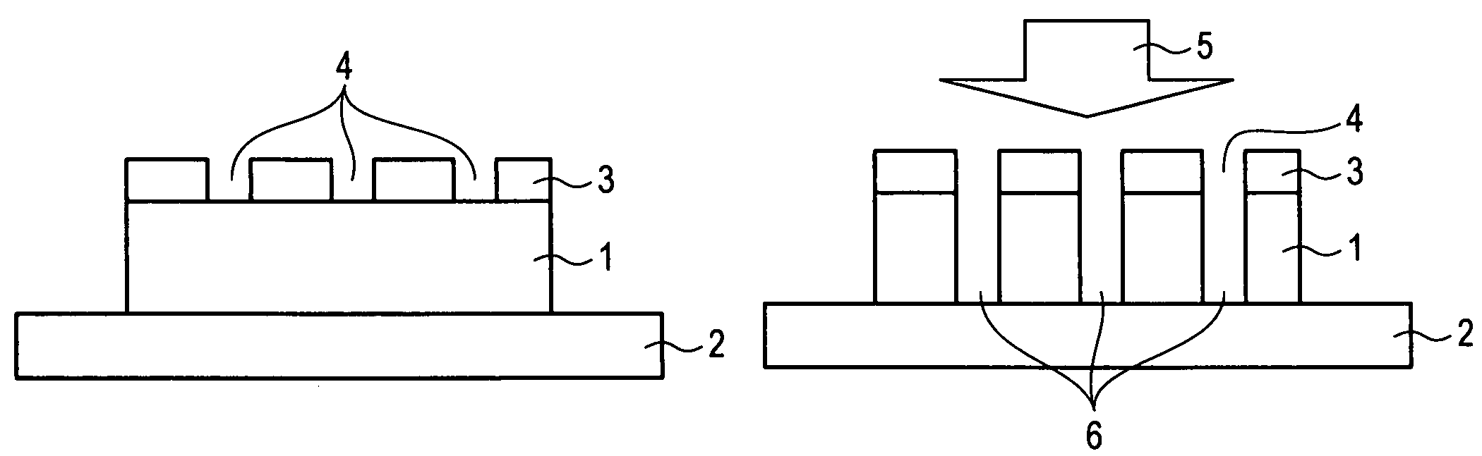
[0075]A porous drawn PTFE film (trade name “HP010-60”, manufactured by SUMITOMO ELECTRIC FINE POLYMER, INC.) with a pore size of 0.1 μm, a porosity (ASTM D-792) of about 50%, and a film thickness of 60 μm was smoothed and placed on a glass plate, and fixed at the edges by a tape made of plastic so as not to move. On the porous drawn PTFE film, an instant adhesive (trade name “Aron Alpha”, manufactured by TOAGOSEI Co., Ltd.) was thinly applied. Then, on the instant adhesive layer, a mask made of a stainless steel with a thickness of 0.05 mm, having a slit with a width of 100 μm and a length of 5 mm opened therein, was placed. The film-was allowed to stand still for a whole day and night, so that the instant adhesive was sufficiently dried, thereby to fix the mask made of a stainless steel on the porous drawn PTFE film.

[0076]From above the mask made of a stainless steel, a sand blast processing by a compressed air was carried out by the use of alumina abrasive grains with an average g...

example 2

[0079]A porous drawn PTFE film (trade name “WP500-100”, manufactured by SUMITOMO ELECTRIC FINE POLYMER, INC.) with a pore size of 5 μm, a porosity of about 80%, and a film thickness of 100 μm was smoothed and placed on a glass plate, and fixed by a tape so as not to move. On the porous drawn PTFE film, an instant adhesive (trade name “Aron Alpha”, manufactured by TOAGOSEI Co., Ltd.) was thinly applied. Then, on the adhesive layer, a mask made of a stainless steel with a thickness of 0.05 mm, having a slit with a width of 100 μm and a length of 5 mm opened therein, was placed. The film was allowed to stand still for a whole day and night, so that the instant adhesive was sufficiently dried, thereby to fix the mask made of a stainless steel on the porous drawn PTFE film.

[0080]From above the mask made of a stainless steel, a sand blast processing by a compressed air was carried out by the use of alumina abrasive grains with an average grain diameter of about 5 μm. By the inspection wit...

example 3

[0083]A porous drawn PTFE film (trade name “WP500-100”, manufactured by SUMITOMO ELECTRIC FINE POLYMER, INC.) with a pore size of 5 μm, a porosity of about 80%, and a film thickness of 100 μm was smoothed and placed on a glass plate, and fixed by a tape so as not to move. On the porous drawn PTFE film, an instant adhesive (trade name “Aron Alpha”, manufactured by TOAGOSEI Co., Ltd.) was thinly applied. Then, on the adhesive layer, a mask made of a stainless steel with a thickness of 0.05 mm, having a slit with a width of 100 μm and a length of 5 mm opened therein, was placed. The film was allowed to stand still for a whole day and night, so that the instant adhesive was sufficiently dried, thereby to fix the mask made of a stainless steel on the porous drawn PTFE film.

[0084]From above the mask made of a stainless steel, a sand blast processing by a compressed air was carried out by the use of sodium chloride abrasive grains with an average grain diameter of about 5 μm. By the inspec...


PUM

PropertyMeasurementUnit
thicknessaaaaaaaaaa
temperatureaaaaaaaaaa
porosityaaaaaaaaaa

Abstract

An object of the present invention is to provide a method for manufacturing a porous material in which complicated and fine through portions, recessed portions, and the like have been patterned. It is to provide a patterned porous molded product or nonwoven fabric, in which a plated layer has been selectively formed on the surfaces of the through portions and the recessed portions.With the invention, a mask having through portions in a pattern is placed on at least one side of the porous molded product or the nonwoven fabric. A fluid or a fluid containing abrasive grains is sprayed from above the mask, thereby to form through portions or recessed portions, or both of them, to which the opening shape of each through portion of the mask has been transferred, in the porous molded product or the nonwoven fabric. The invention provides a porous molded product or a nonwoven fabric in which a plated layer has been selectively formed on the surfaces of the through portions or the recessed portions, or both of these, an electric circuit component, or the like.

Description

RELATED APPLICATION[0001]This application is a national phase of PCT / JP2005 / 000623 filed on Jan. 13, 2005, which claims priority from Japanese Application No. JP 2004-007043 filed on Jan. 14, 2004, the disclosures of which Applications are incorporated by reference herein. The benefit of the filing and priority dates of the International and Japanese Applications is respectfully requested.TECHNICAL FIELD[0002]The present invention relates to a method for manufacturing a porous molded product or a nonwoven fabric in which through portions such as through holes and through trenches, and recessed portions such as trenches have been patterned. Further, the invention relates to a method for manufacturing a porous molded product or a nonwoven fabric in which a plated layer has been selectively formed on the surfaces of the recessed portions or the through portions formed by patterning, or both of these. Still further, the invention relates to an electric circuit component made of a porous...

Claims


Application Information

Patent Timeline
Patent Type & Authority Patents(United States)
IPC IPC(8): H05K1/11B31D3/00C23C18/22B24C1/04B24C3/32B24C11/00C23C18/16H05K1/00H05K3/10H05K3/18
CPCB24C1/04B24C11/00H05K3/107H05K3/184C23C18/1644C23C18/1651B24C3/322Y10T428/24479H05K1/0284H05K3/182H05K2201/0116H05K2201/015H05K2201/0209H05K2201/0293H05K2201/09036H05K2201/09118H05K2203/025H05K2203/0565C23C18/1605C23C18/1653C23C18/30Y10T428/24612Y10T428/24496Y10T428/249953Y10T428/249987Y10T442/674C23C18/16H05K3/10
Inventor HAYASHI, FUMIHIROMASUDA, YASUHITOOKUDA, YASUHIRO
Owner SUMITOMO ELECTRIC IND LTD
Why Eureka
Try Eureka