
Measurement of corner roundness

a technology of roundness and measurement, applied in the field of image processing, can solve the problem of not being able to provide accurate curvature measurements when applied to image features with noisy edges, and achieve the effect of reducing noise and reducing nois

Active Publication Date: 2009-09-15
APPLIED MATERIALS INC
View PDF14 Cites 2 Cited by
  • Summary
  • Abstract
  • Description
  • Claims
  • Application Information

AI Technical Summary

Benefits of technology

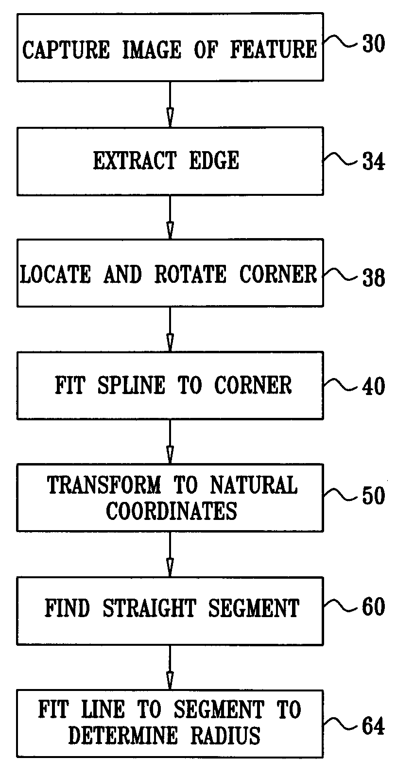
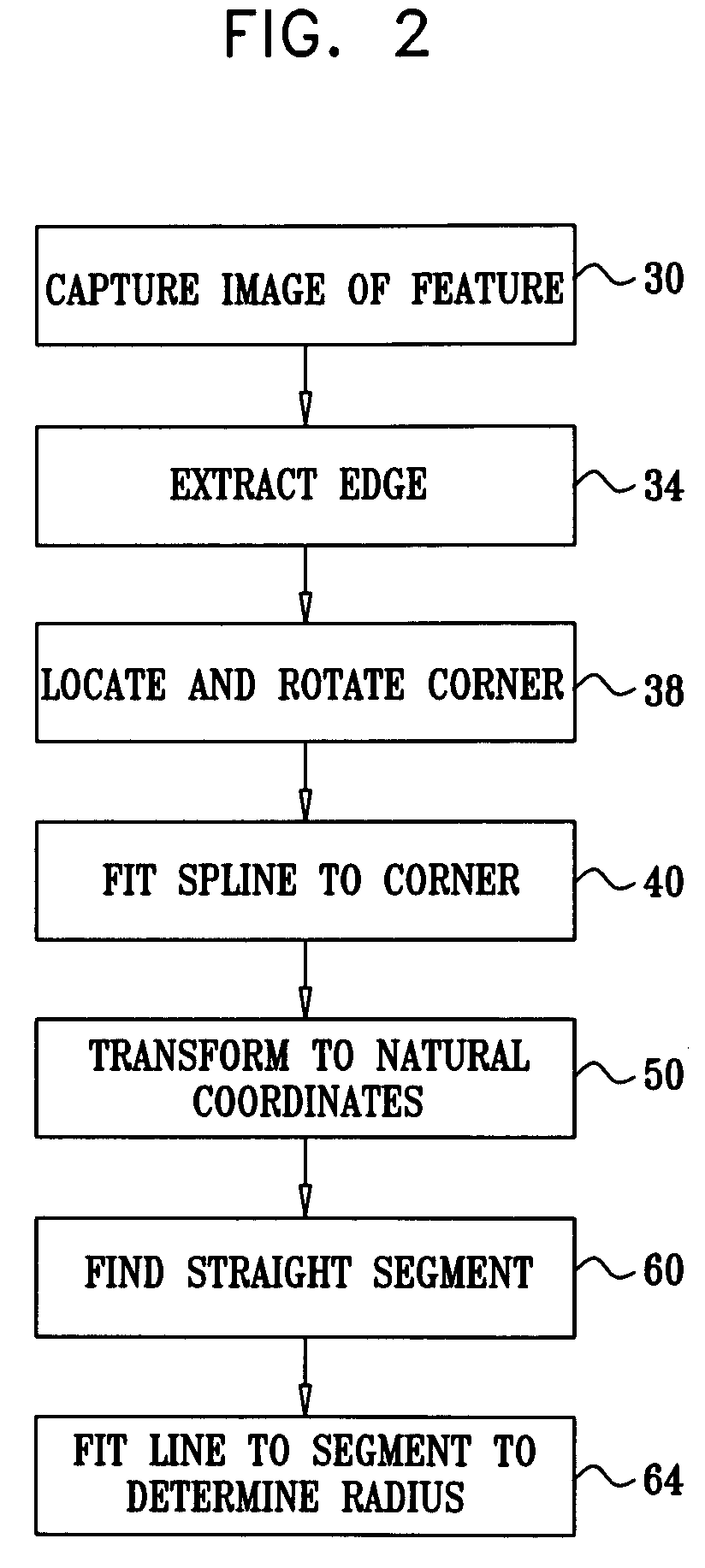
The present invention provides improved methods and systems for automatic curvature measurement, particularly for image features with noisy edges. These methods involve identifying curved segments of a contour, smoothing them to reduce noise, and then transforming them to a natural coordinate system. A line is then fitted to the transformed segment to determine the radius of curvature of the curved segment. These methods are reliable even in the presence of substantial noise and are useful in various areas of image processing, such as semiconductor wafers and reticles.

Problems solved by technology

Although various methods for curvature analysis are known in the art, and may work adequately in some cases, these methods often fail to provide accurate curvature measurements when applied to image features that have noisy edges, i.e., edges that are characterized by random, high-frequency fluctuations.

Method used


Image

  • Measurement of corner roundness
  • Measurement of corner roundness
  • Measurement of corner roundness

Examples


Embodiment Construction

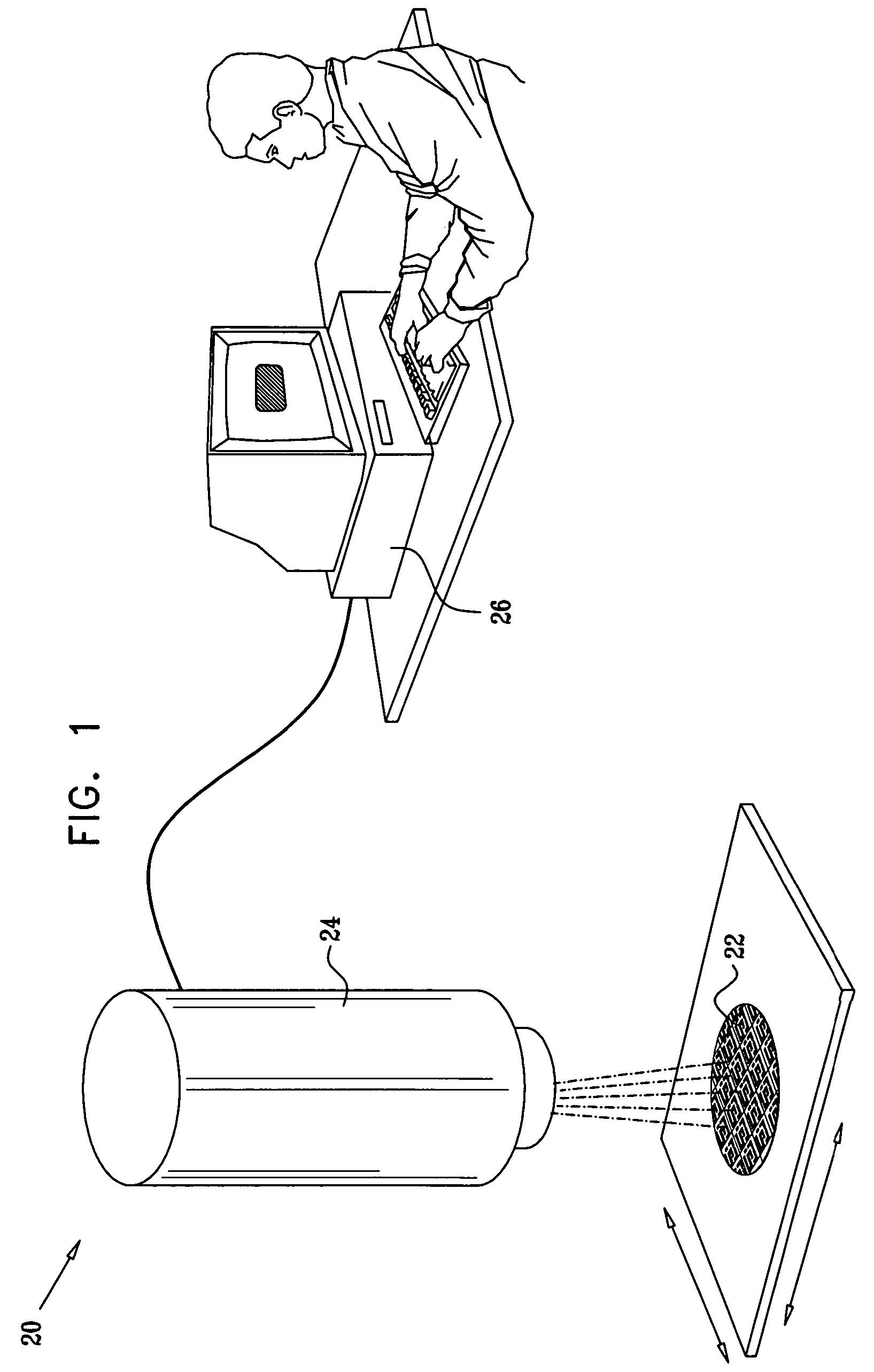
[0029]FIG. 1 is a schematic pictorial illustration of a system 20 for inspection of a sample 22, such as a semiconductor wafer, in accordance with an embodiment of the present invention. System 20 is built around means for providing high-resolution images of the sample. Typically, the means comprise a SEM 24, which images an area of sample 22 using a scanning electron beam. The sample may be mounted on a translation stage (not shown), to permit different areas of the sample surface to be imaged. Alternatively or additionally, the means for providing the high-resolution images may comprise a data storage device, which stores and recalls the images as required.

[0030]The images of sample 22 are input to an image processor 26 for image enhancement and analysis. The image processor may be a standalone unit, as shown in FIG. 1, or it may be integrated into a single unit with the SEM itself. Typically, processor 26 comprises a general-purpose computer, which is programmed in software to ca...


PUM


Abstract

A method for analyzing an image includes identifying a curved segment of a contour that is associated with noise. The curved segment is smoothed so as to reduce the noise that is associated with the curved segment, thereby providing a smoothed segment. The smoothed segment is transformed to a natural coordinate system, thereby providing a transformed segment. A line is fitted to the transformed segment in order to determine a radius of curvature of the curved segment.

Description

CROSS-REFERENCE TO RELATED APPLICATION[0001]This application claims the benefit of U.S. provisional patent application 60 / 493,518, filed Aug. 8, 2003, which is incorporated herein by reference.FIELD OF THE INVENTION[0002]The present invention relates generally to image processing, and specifically to measuring the roundness of corners of a structure in an image, such as rectangular structures in a microscopic image of a semiconductor wafer or reticle.BACKGROUND OF THE INVENTION[0003]Structures in reticles and in layers produced on semiconductor wafers by photolithography are generally designed to have square corners. In practice, however, the limitations inherent in fabrication techniques inevitably result in some rounding of the corners. Such rounding may have adverse effects on the performance of microcircuits that incorporate the structures. For example, rounding of the corners of a contact pad reduces the effective contact area and may thus increase the contact resistance. The e...

Claims


Application Information

Patent Timeline
Patent Type & Authority Patents(United States)
IPC IPC(8): G06K9/00G06T5/00G06T7/00G06T7/60
CPCG06T7/0004G06T7/0083G06T7/604G06T2207/30148G06T2207/10061G06T7/12G06T7/64
Inventor ROMAN, KRISMENADEVA, OVADYATAM, AVIRAMGOTTLIB, GIDIGERSHTEIN, LIRAZ
Owner APPLIED MATERIALS INC
Learn More