Input cancellation circuit

a cancellation circuit and input technology, applied in the field of input cancellation circuits, can solve the problems of significant parasitic capacitance, significant distortion during normal operation, and reduce the bandwidth of the input circui

Active Publication Date: 2009-10-13
ANALOG DEVICES INC
View PDF3 Cites 2 Cited by
  • Summary
  • Abstract
  • Description
  • Claims
  • Application Information

AI Technical Summary

Problems solved by technology

However, if the series switch resistance is allowed to dominate over the input resistor, it may result in significant distortion during normal operation due to non-linear junction capacitances.
If the series switch resistance is made small with respect to the low input resistance, the large physical size of the switch can introduce significant parasitic capacitance and reduce the bandwidth of the input circuits.
Furthermore, if the input is allowed to exceed the supply voltage by more than the gate oxide breakdown of the series switch, then when the series switch is isolated, the oxide of the switch may be exposed to damage.
The NFET used as a switch 140 can add substantial distortion during normal operation due to its non-linear junction capacitance.
However, as the size of the NFET 140 increases, the parasitic capacitance of the device increases with it, thereby reducing the bandwidth of the input circuits.
Furthermore, if the input 110 is allowed to exceed the supply voltage by more than the gate oxide breakdown of the NFET 140, then when the NFET 140 is isolated, the oxide of the NFET may be exposed to damage.

Method used


Image

  • Input cancellation circuit
  • Input cancellation circuit
  • Input cancellation circuit

Examples


Embodiment Construction

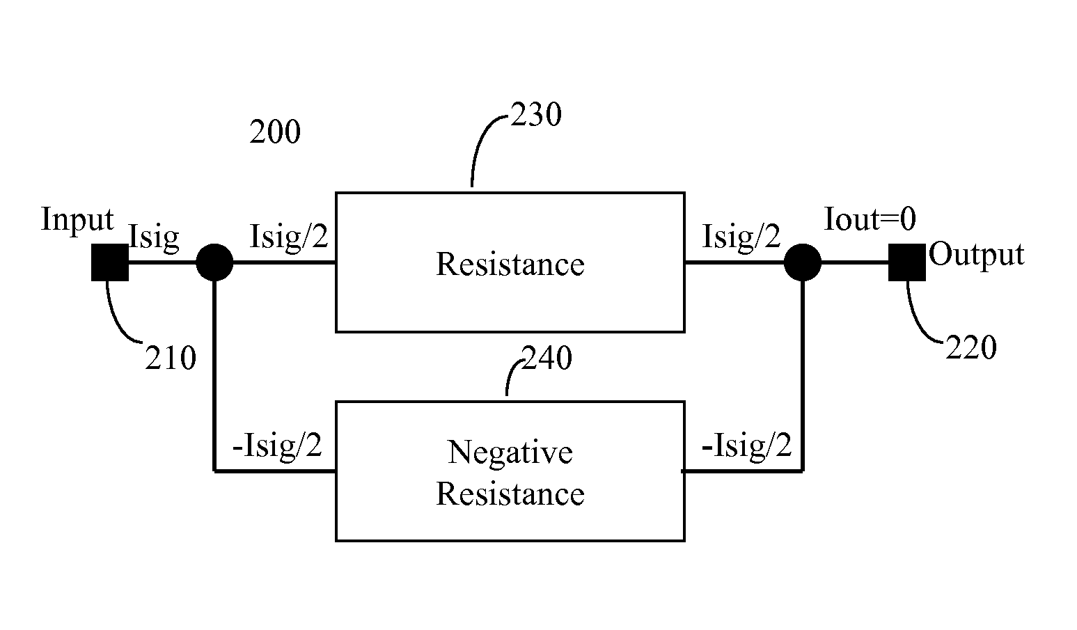
[0016]A system and method is provided for effectively isolating an input from a circuit. FIG. 2 shows a block diagram of a single ended isolation method in accordance with an embodiment of the invention. An input 210 is coupled to an input resistance 230 and a negative resistance 240. The outputs of resistance 230 and negative resistance 240 are coupled to output 220. By making the negative resistance path 240 substantially equal in magnitude to the resistance 230, the signal at input 210 is effectively cancelled. For example, the current through resistance 230 Isig / 2 and the current through the negative resistance 240 Isig / 2 is equal but opposite in direction. Therefore, the current at the output 220 is 0, thereby effectively canceling the signal at input 210. These relationships are summarized by the following equations:

[0017]Iout=VInput-VOutputR⁢-RR⁢-R=-R×RR+(-R)If⁢⁢R=-R❘then,⁢R⁢-R=∞,⁢and⁢⁢Iout=0

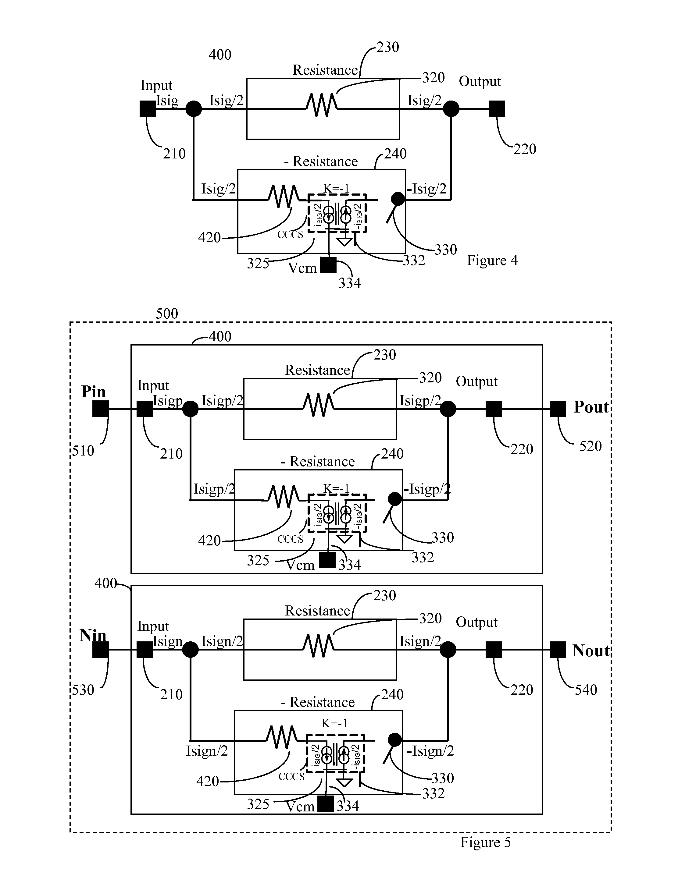
[0018]As illustrated in FIG. 4, the input resistance 230 may comprise a resistor 320....


PUM


Abstract

A system and method are provided for isolating an input without adding significant distortion and without significantly adversely affecting the bandwidth of input circuits. In one embodiment, a single ended signal is substantially cancelled by an arrangement including an input resistance path in parallel with a negative resistance path wherein both paths substantially match in resistance. In another embodiment, a differential signal is substantially cancelled by a pseudo differential arrangement including two independent input resistance paths each in parallel with a corresponding negative resistance path, wherein the resistance paths substantially match the input resistance paths. In yet another embodiment, a differential signal is substantially cancelled by a differential arrangement including two resistance paths wherein a first negative resistance path is coupled between the first differential input and the second differential output and the second negative resistance path is coupled between the second input and the first output. In yet another embodiment, a current controlled current source may provide the negative amplification for the negative resistance path.

Description

COPYRIGHT AND LEGAL NOTICES[0001]A portion of the disclosure of this patent document contains material which is subject to copyright protection. The copyright owner has no objection to the facsimile reproduction by anyone of the patent document or the patent disclosure, as it appears in the Patent and Trademark Office patent files or records, but otherwise reserves all copyrights whatsoever.BACKGROUND INFORMATION[0002]The present invention relates in general to input cancellation circuits, and more particularly to input cancellation in resistively coupled circuits.[0003]Low noise resistively coupled circuits may need a small input resistor to ensure that the noise contribution of the input resistor does not dominate the overall noise of the system. The system may need to be isolated, for example, for calibration purposes. To isolate the input, a series switch may be used. However, if the series switch resistance is allowed to dominate over the input resistor, it may result in signif...

Claims


Application Information

Patent Timeline
Patent Type & Authority Patents(United States)
IPC IPC(8): G01R1/20
CPCH03F3/45179H03K17/063H03H11/38H03F2200/91H03F2203/45306H03H11/52H03F2203/45682
Inventor SCHOFIELD, WILLIAM GEORGE JOHNSINGER, LAWRENCE A.
Owner ANALOG DEVICES INC
Why Eureka
Try Eureka