Display device and method for fabricating the same

Inactive Publication Date: 2009-11-03
SEMICON ENERGY LAB CO LTD
View PDF86 Cites 45 Cited by
  • Summary
  • Abstract
  • Description
  • Claims
  • Application Information

AI Technical Summary

Benefits of technology

[0012]In accordance with the present invention, in order to reduce a fabrication cost of an active-matrix type display device, all of the TFTs to be used in a pixel section are provided as a TFT of one conductivity type (indicating herein either a p-channel

Problems solved by technology

Although in the developments for the light-emitting devices the passive-matrix type devices have been mainly focused, it has been considered that there will exist disadvantages with the passive-matrix type light-emitting devices in that a sufficient reliability (a long lifetime of the EL element) cannot be ensured with a higher precision pixel section which requires the luminance of the EL element to be increased.
However, it is difficult to ensure a sufficient production yield of the active-matrix type light-emitting device, as compared to the passive-matrix type device that has a simpler structure, since a plurality of TFTs have to be formed

Method used


Image

  • Display device and method for fabricating the same
  • Display device and method for fabricating the same
  • Display device and method for fabricating the same

Examples


embodiment 1

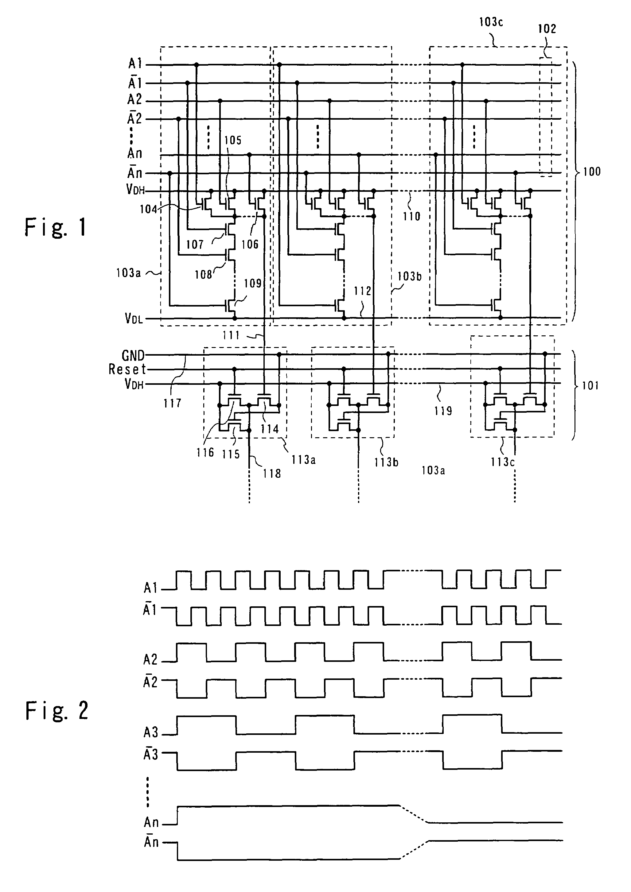
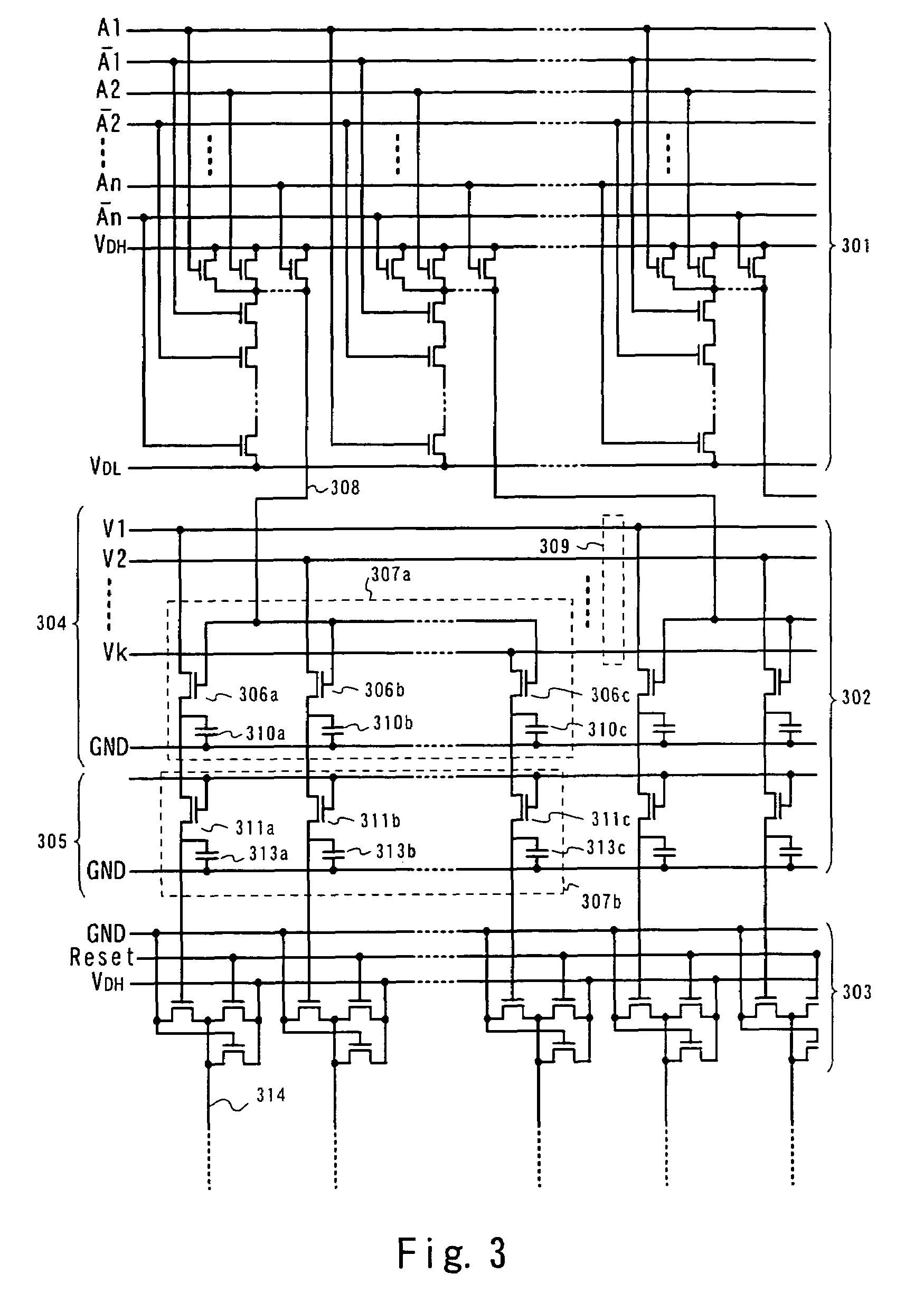
[0063]In the present invention, the pixel section, in addition to the driver circuit, is entirely composed of the p-channel TFTs. Thus, in the present embodiment, the structure of the pixel section for displaying an image in accordance with the signals transmitted by the driver circuit as shown in FIGS. 1 and 3 will be described.

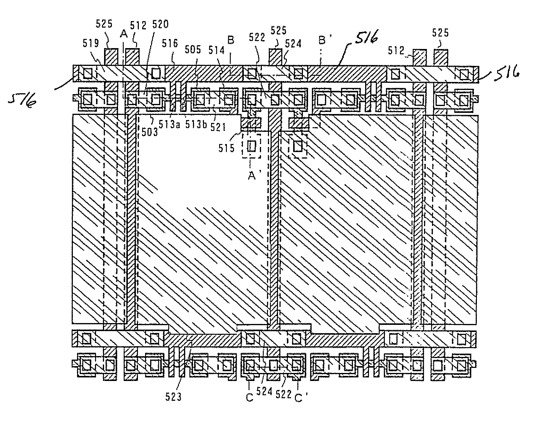
[0064]The structure of a pixel of an active-matrix type light-emitting device in accordance with the present invention is shown in FIGS. 5 and 6. FIG. 5 illustrates a cross-sectional view of one pixel, while FIG. 6 illustrates a top view of adjacent two pixels. FIG. 5 shows a cross-sectional view cut along A-A′ in FIG. 6, and the same component is designated with the same reference numeral in both of these figures. In addition, the two pixels illustrated in FIG. 6 are symmetric to each other with respect to the current supply line 525, and therefore, have the same structure as each other.

[0065]In FIG. 5, reference numeral 501 denotes a substrate transparent ...

embodiment 2

[0081]In the present embodiment, the fabrication process of an active-matrix type light-emitting device in which a pixel section and a driver circuit for transmitting a signal to the pixel section are formed on the identical insulating surface will be described with reference to FIGS. 8(A) to 8(D) and FIGS. 9(A) to 9(C).

[0082]First, as shown in FIG. 8(A), an underlying film (insulating body) 802 is formed on a glass substrate 801. In the present embodiment, the underlying film 802 is formed by sequentially depositing a first silicon oxynitride film having a thickness of 50 nm and a second silicon oxynitride film having a thickness of 200 nm in this order from the side closer to the glass substrate 801. The nitrogen content of the first silicon oxynitride film is larger than that of the second silicon oxynitride film so as to suppress diffusion of alkali metal from the glass substrate 801.

[0083]Then, an amorphous silicon film (not shown) is formed on the underlying film 802 by a plas...

embodiment 3

[0107]In Embodiment 2 mentioned in the above, the circuit structure of the pixel section shown in FIG. 10 can be modified as shown in FIG. 11. Specifically, in FIG. 11, reference numeral 1101 denotes a source wiring, 1102 denotes a gate wiring, 1103 denotes a switching TFT, 1104 denotes a current-controlling TFT, 1105 denotes a current supply line, and 1106 denotes an EL element. In the present embodiment, each of the switching TFT 1103 and the current-controlling TFT 1104 is formed as the p-channel TFT.

[0108]In this case, since the gate wiring 1102 and the current supply line 1105 are disposed in different layers, it is advantageous to provide these components so as to overlap each other with an interlayer insulating film interposed therebetween. Thus, an occupied area of these lines can be substantially made common, and therefore, the effective light-emission area of the pixel can be increased.


PUM


Abstract

An inexpensive display device, as well as an electrical apparatus employing the same, can be provided. In the display device in which a pixel section and a driver circuit are included on one and the same insulating surface, the driver circuit includes a decoder 100 and a buffer section 101. The decoder 100 includes a plurality of NAND circuits each including p-channel TFTs 104 to 106 connected to each other in parallel and other p-channel TFTs 107 to 109 connected to each other in series. The buffer section 101 includes a plurality of buffers each including three p-channel TFTs 114 to 116.

Description

BACKGROUND OF THE INVENTION[0001]1. Field of the Invention[0002]The present invention relates to a device having an element in which a light-emitting material is interposed between electrodes (hereinafter, such a device is referred to as the light-emitting device and such an element is referred to as the light-emitting element). In particular, the present invention relates to a device including on one and the same insulating surface, a pixel section and a driver circuit for transmitting a signal to the pixel section. In addition, the present invention can be used for a device having an element in which liquid crystal is interposed between electrodes (hereinafter, such a device is referred to as the liquid crystal display device and such an element is referred to as the liquid crystal element). It should be noted that in the present specification, the light-emitting device and the liquid crystal display device are collectively referred to as the display device.[0003]Light-emitting ma...

Claims


Application Information

Patent Timeline
IPC IPC(8): G09G3/36G02F1/1333G02F1/133G02F1/1362G09F9/30G09G3/32H01L21/00H01L21/84H01L27/12H01L27/15H01L27/32H01L31/12H05B33/00
CPCG02F1/136286G09G3/3233G09G3/3266G09G3/3291G09G3/3648H01L27/3276H01L27/1248H01L27/1222H01L27/124H01L2924/0002G09G2300/0842G09G2300/0861G09G2310/027H01L2924/00Y02E10/549Y02P70/50H10K59/35H10K59/131G02F1/133H10K50/844H10K50/841H10K59/123H10K59/1315H10K77/111H10K2102/00H10K2102/311
Inventor KOYAMA, JUN
Owner SEMICON ENERGY LAB CO LTD
Why Eureka
Try Eureka