High-speed RFID circuit placement method and device

a technology of rfid circuit and placement method, which is applied in the direction of burglar alarm mechanical actuation, burglar alarm by hand-portable object removal, instruments, etc., can solve the problems of reducing the accuracy required for the placement of chips, increasing complexity and thickness of rfid devices, and affecting the accuracy of rfid devices

Active Publication Date: 2009-11-24
AVERY DENNISON CORP
View PDF276 Cites 63 Cited by
  • Summary
  • Abstract
  • Description
  • Claims
  • Application Information

AI Technical Summary

Benefits of technology

[0021]In another exemplary embodiment, a machine is provided for making an RFID device including a web advancement device configured to advance a web of RFID circuits through an RFID circuit separation device, and a scrap web removal device downstream of the RFID circuit separation device. The web advancement device and scrap web removal device are configured to cooperatively advance the web of RFID circuits through the RFID circuit separation device to prevent buckling of the web of RFID circuits as the web of RFID circuits passes through the RFID circuit separation device.

Problems solved by technology

Structures for these purposes can add complexity, thickness and inflexibility to an RFID device.
These machines are relatively slow, and usually require an intermittent indexing process whereby the antenna web stops for a short period of time while the chip is placed onto an antenna on the antenna web.
The larger coupling area provided by the interposer effectively reduces the accuracy required for the placement of a chip during manufacture while still providing an effective electrical connection between the chip and an antenna.
Chip placement and mounting are serious limitations for high-speed manufacture.
However, the web speed and production rate are still quite low.
Some of the difficulty arises from the difference in spacing of the straps or interposers on the carrier web, and the spacing of the antenna structures to which the interposers will be attached.

Method used


Image

  • High-speed RFID circuit placement method and device
  • High-speed RFID circuit placement method and device
  • High-speed RFID circuit placement method and device

Examples


Embodiment Construction

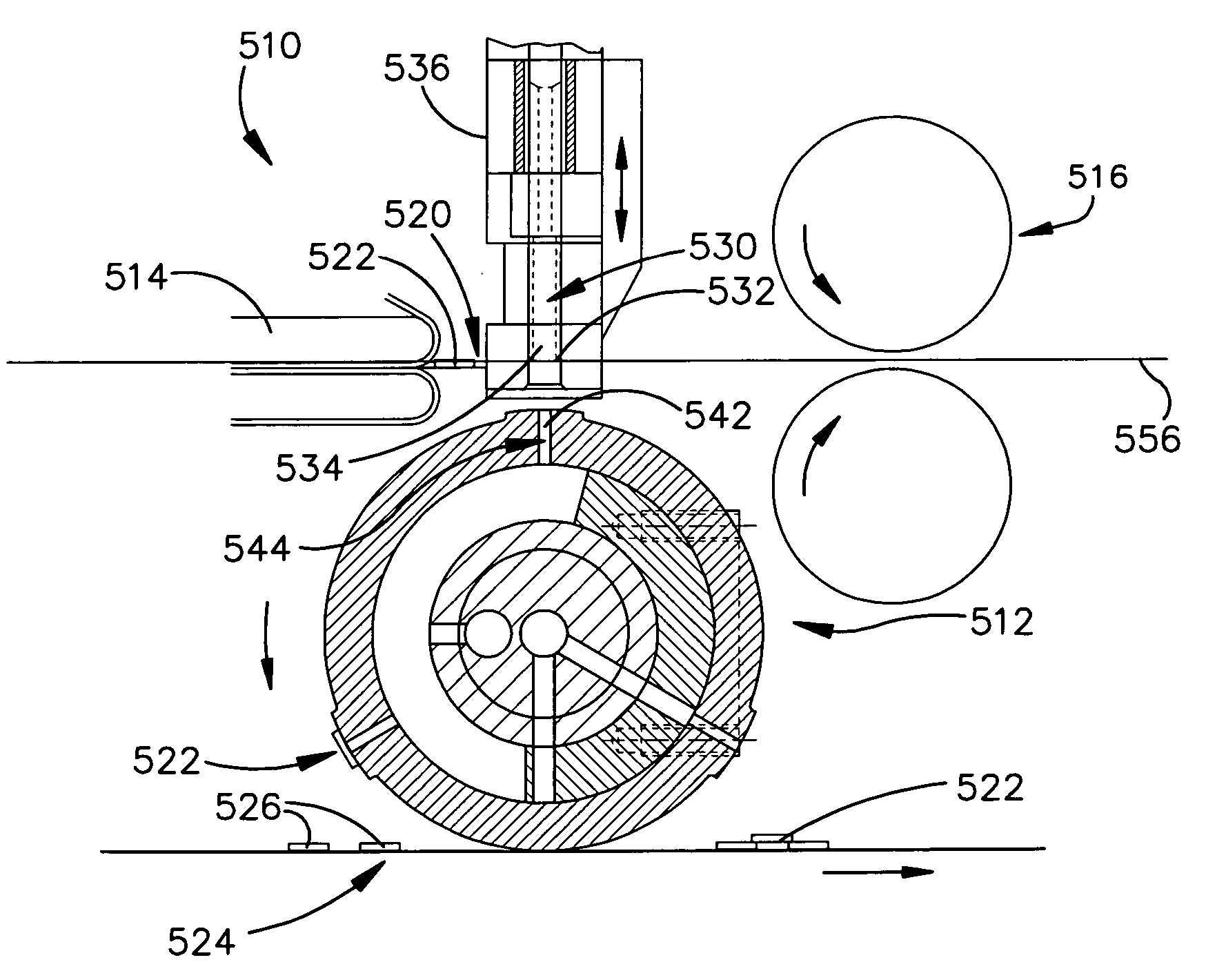
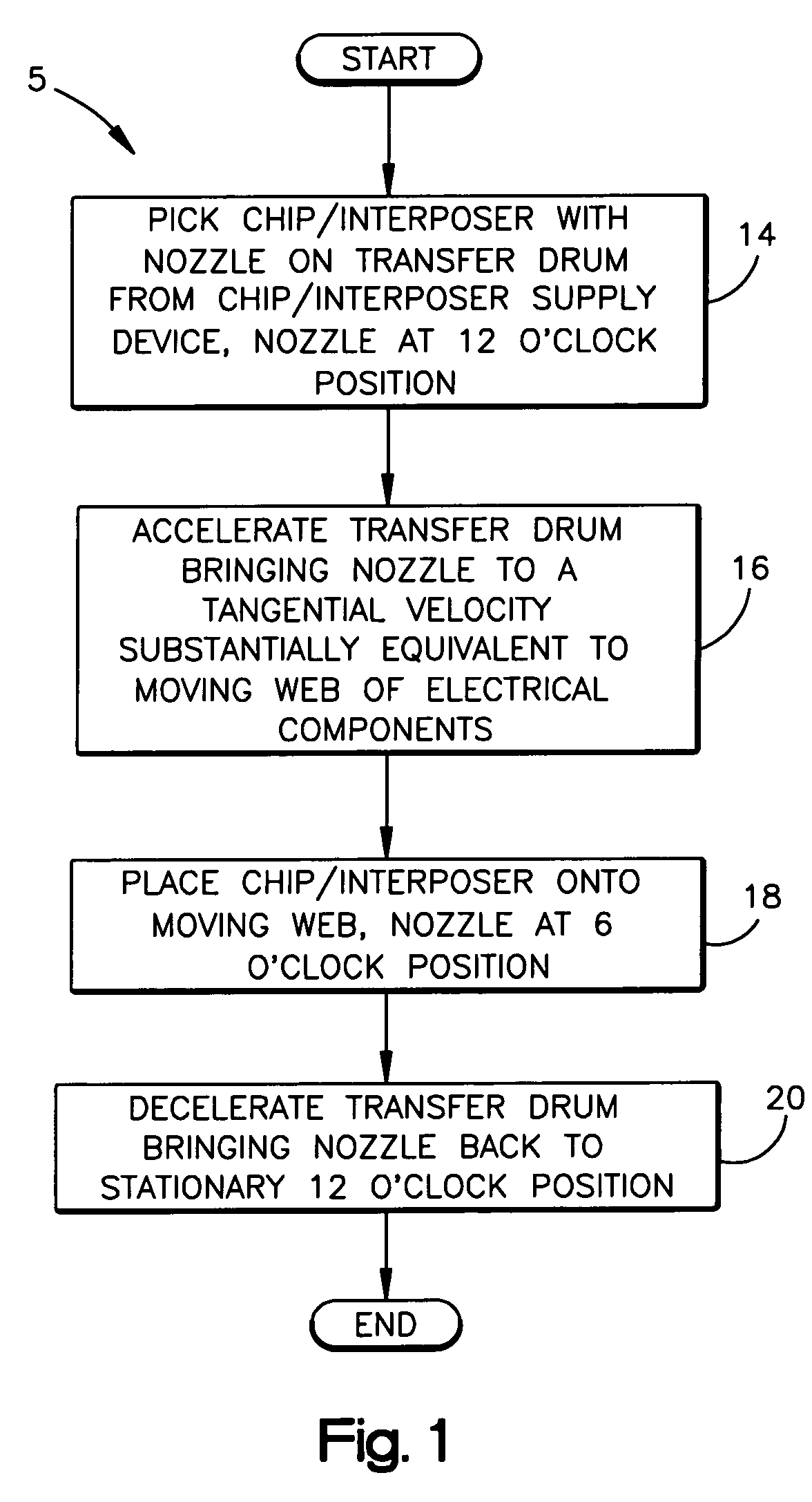
[0038]A high-speed machine and method for placing an RFID circuit onto an electrical component includes separating an RFID circuit from a web of RFID circuits, and placing the RFID circuit onto an electrical component with a placing device. The separating includes directing the RFID circuit onto a transfer drum of the placement device and separably coupling the RFID circuit to the transfer drum. According to one method, a separator device separates and directs chips or interposers onto a placement device. According to another method, chips or interposers are tested before being separated from a web, and if good, are separated from the web, directed onto a placement device, and placed on an electrical component. If defective, the chips or interposers are not directed onto a placement device and are removed by a scrap web removal device.

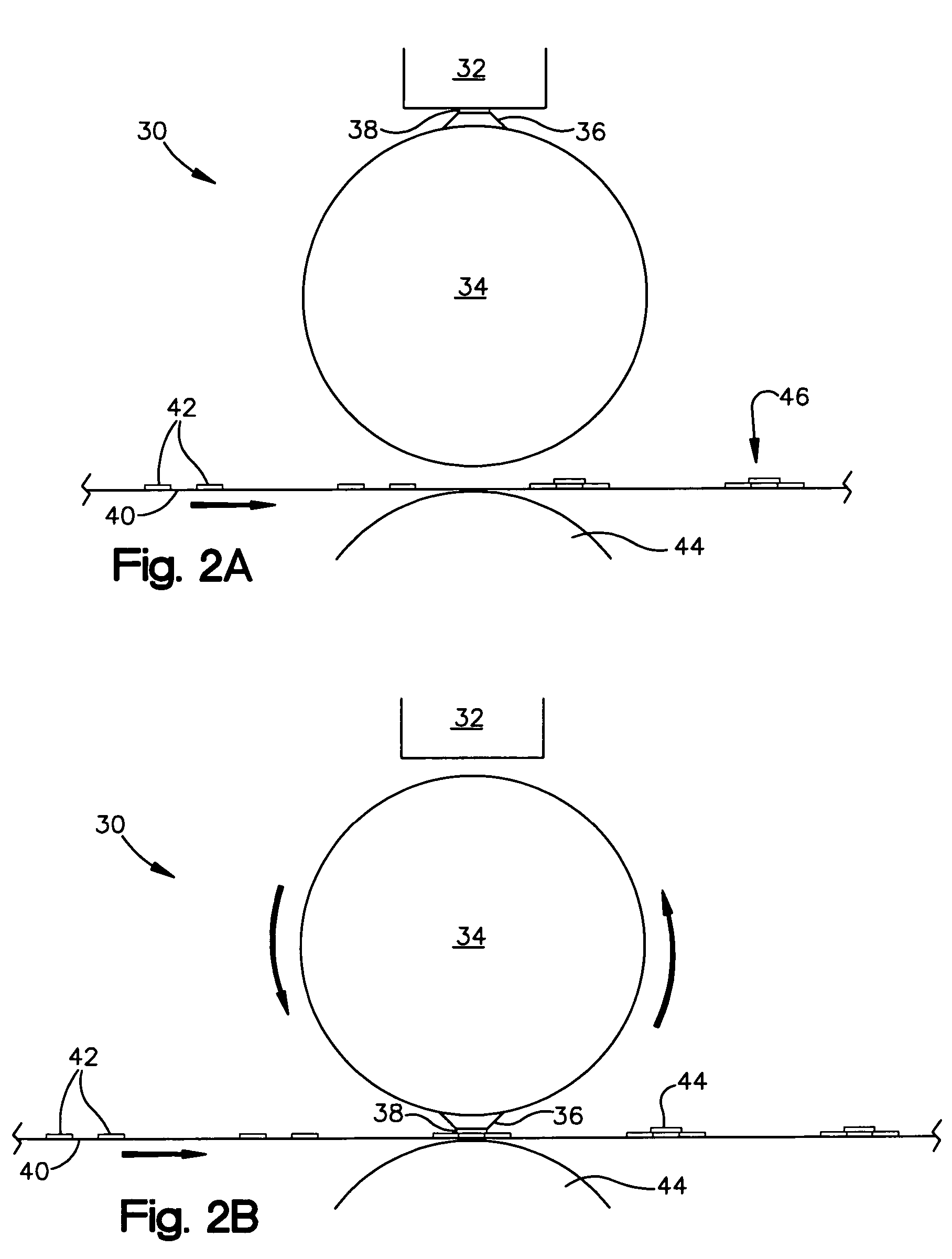
[0039]In FIG. 1, a flow chart is shown depicting a method 5 of placing an RFID circuit onto an antenna disposed on a moving web. The method 5 of FIG. ...


PUM

PropertyMeasurementUnit
distanceaaaaaaaaaa
distanceaaaaaaaaaa
thicknessaaaaaaaaaa

Abstract

A high-speed machine and method for placing an RFID circuit onto an electrical component includes separating an RFID circuit from a web of RFID circuits, and placing the RFID circuit onto an electrical component with a placing device. The separating includes directing the RFID circuit onto a transfer drum of the placement device and separably coupling the RFID circuit to the transfer drum. According to one method, a separator device separates and directs chips or interposers onto a placement device. According to another method, chips or interposers are tested before being separated from a web, and if good, are separated from the web, directed onto a placement device, and placed on an electrical component. If defective, the chips or interposers are not directed onto a placement device and are removed by a scrap web removal device.

Description

RELATED APPLICATIONS[0001]This application claims the benefit of U.S. Provisional Application No. 60 / 674,429 filed Apr. 25, 2005, which is hereby incorporated herein by reference. This application is related to U.S. application Ser. No. 10 / 947,010 filed on Sep. 22, 2004.BACKGROUND OF THE INVENTION[0002]1. Field of the Invention[0003]The present invention relates generally to the assembly of electronic devices. More particularly, the present invention relates to the assembly of radio frequency identification (RFID) interposers, inlays, tags and labels.[0004]2. Description of the Related Art[0005]Radio frequency identification (RFID) tags and labels (collectively referred to herein as RFID “devices”) are widely used to associate an object with an identification code. RFID devices generally have a combination of antennas and analog and / or digital electronics, which may include, for example, communications electronics, data memory, and control logic. RFID devices typically further inclu...

Claims


Application Information

Patent Timeline
Patent Type & Authority Patents(United States)
IPC IPC(8): G08B13/14
CPCG06K7/0095G06K19/07718G06K19/07749G06K19/07752G06K19/07756H01L21/67144H01L21/67271Y10T29/49133H01L2224/75822Y10T29/49018Y10T29/4913Y10T29/49137Y10T29/49004G06K19/07G06K19/077
Inventor FERGUSON, SCOTT WAYNELINKMANN, RALFKIEHNE, WERNER
Owner AVERY DENNISON CORP
Why Eureka
Try Eureka