FinFET with sublithographic fin width

a finfet and sublithographic technology, applied in the field of sublithographic fin fin structure of finfet, can solve the problems of gate length scaling down and the width of finfet facing ever more difficulties

Active Publication Date: 2009-12-01
INT BUSINESS MASCH CORP
View PDF3 Cites 119 Cited by
  • Summary
  • Abstract
  • Description
  • Claims
  • Application Information

AI Technical Summary

Problems solved by technology

While scaling down of the gate length of finFETs faces difficulties due to lithographic limitations, scaling down of the width of the finFETs faces ever more difficulties since the width of the fin needs to have an even smaller dimension than the gate length of the finFET.

Method used


Image

  • FinFET with sublithographic fin width
  • FinFET with sublithographic fin width
  • FinFET with sublithographic fin width

Examples


Embodiment Construction

[0062]As stated above, the present invention relates to finFET structures having a sublithographic fin width and methods of manufacturing the same, which are now described in detail with accompanying figures. It is noted that like and corresponding elements are referred to by like reference numerals.

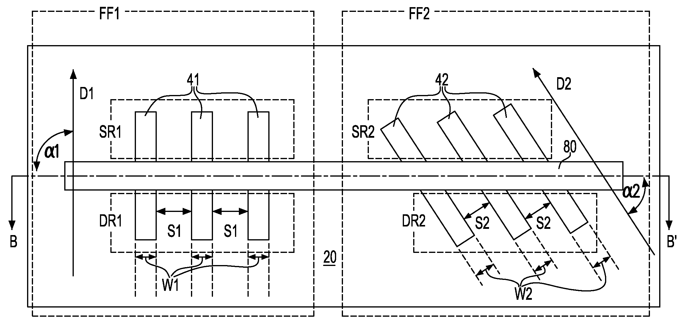
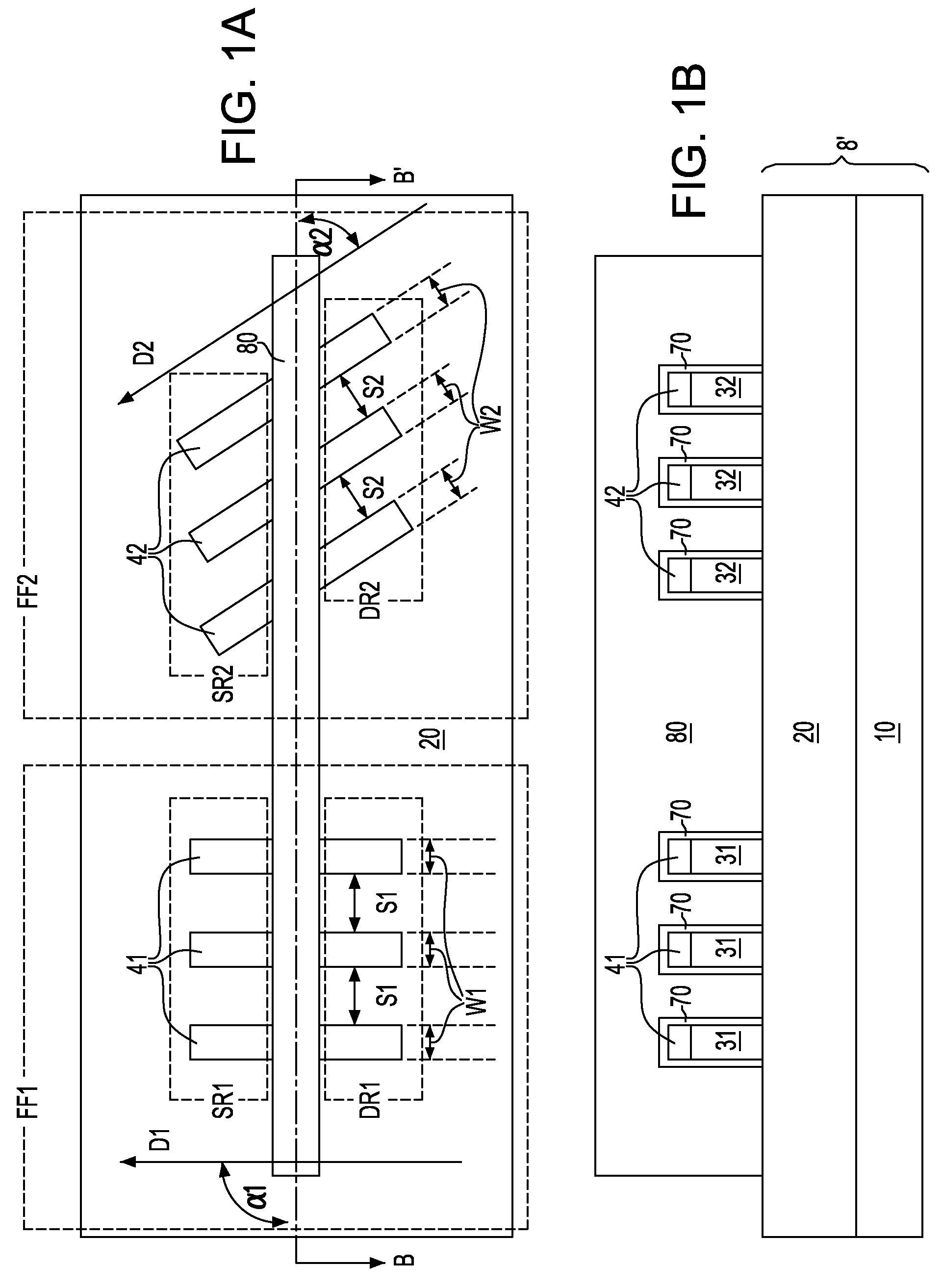
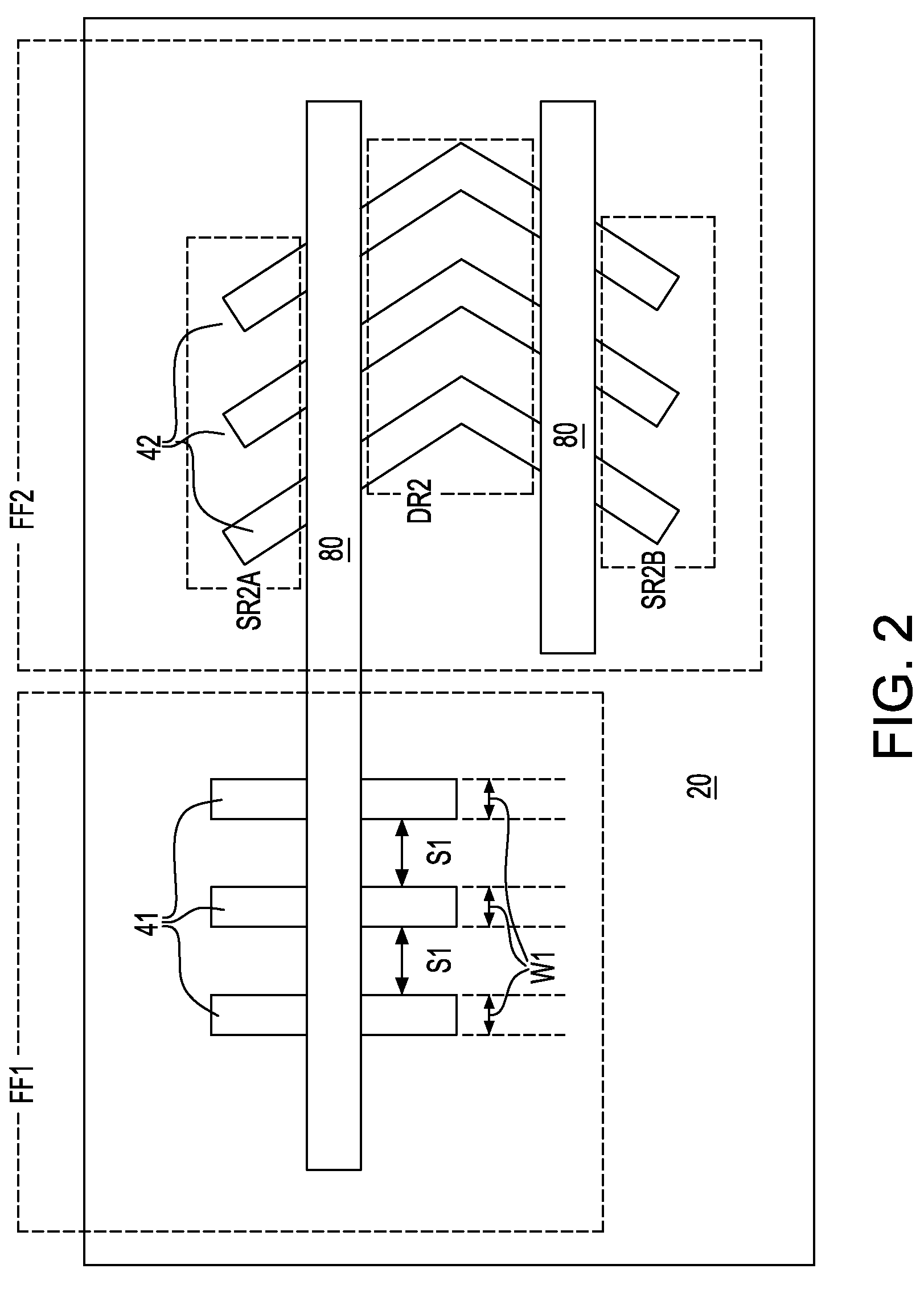
[0063]Referring to FIGS. 1A and 1B, a first exemplary structure according to the present invention is shown, which comprises a substrate 8′ comprising a handle substrate 10 and a buried insulator layer 20. First semiconductor fins 31 and second semiconductor fins 32 are formed on the buried insulator layer 20. First semiconductor fins 31 having a first sublithographic width W1 and separated by a first sublithographic spacing S1 are present on the buried insulator layer 20. Similarly, second semiconductor fins 32 having a second sublithographic width W2 and separated by a second sublithographic spacing S2 are present on the buried insulator layer 20 as well. First fin caps 41 and second f...


PUM


Abstract

At least one recessed region having two parallel edges is formed in an insulator layer over a semiconductor layer such that the lengthwise direction of the recessed region coincides with optimal carrier mobility surfaces of the semiconductor material in the semiconductor layer for finFETs to be formed. Self-assembling block copolymers are applied within the at least one recessed region and annealed to form a set of parallel polymer block lines having a sublithographic width and containing a first polymeric block component. The pattern of sublithographic width lines is transferred into the semiconductor layer employing the set of parallel polymer block lines as an etch mask. Sublithographic width semiconductor fins thus formed may have sidewalls for optimal carrier mobility for p-type finFETs and n-type finFETs.

Description

FIELD OF THE INVENTION[0001]The present invention relates to semiconductor structures, and particularly to finFET structures having a sublithographic fin width and methods of manufacturing the same.BACKGROUND OF THE INVENTION[0002]A FinFET is a metal oxide semiconductor field effect transistor (MOSFET) formed on a semiconductor fin. FinFET technology is an emerging technology which provides solutions to metal-oxide-semiconductor field effect transistor (MOSFET) scaling problems at, and below, the 45 nm node. FinMOSFET structures include fin field effect transistors (finFETs), which comprise at least one narrow (preferably <10 nm wide) semiconductor fin gated on at least two opposing sides of each of the at least one semiconductor fin. FinFET structures are preferably formed on a semiconductor-on-insulator (SOI) substrate, because of low source / drain diffusion to substrate capacitance and ease of electrical isolation by shallow trench isolation structures.[0003]A gate electrode is...

Claims


Application Information

Patent Timeline
Patent Type & Authority Patents(United States)
IPC IPC(8): H01L29/00
CPCH01L21/845H01L27/1211H01L29/785H01L29/66795H01L29/045
Inventor YANG, HAINING S.
Owner INT BUSINESS MASCH CORP
Why Eureka
Try Eureka