Multi-layer electronic component and method for manufacturing the same, multi-layer piezoelectric element

a piezoelectric element and electronic component technology, applied in piezoelectric/electrostrictive/magnetostrictive devices, piezoelectric/electrostriction/magnetostriction machines, electrical apparatuses, etc., can solve the problems of reducing the piezoelectric displacement, affecting the stability of the piezoelectric element, etc., to achieve excellent durability, increase the bonding strength, and suppress delamination

Active Publication Date: 2009-12-15
KYOCERA CORP
View PDF34 Cites 16 Cited by
  • Summary
  • Abstract
  • Description
  • Claims
  • Application Information

AI Technical Summary

Benefits of technology

[0022]Particularly, it is an object of the present invention is to provide a multi-layer piezoelectric element that has excellent durability in which delamination is restricted from occurring during operation and the amount of displacement does not vary even when the piezoelectric actuator is subjected to continuous operation over a long period under a high voltage and a high pressure, and an injection apparatus using the same.
[0043]The multi-layer piezoelectric element of the present invention, since the amount of displacement does not substantially change in continuous operation, enables it to constitute the injection apparatus of excellent durability and high reliability that includes the multi-layer piezoelectric element and is capable of operating without failure.

Problems solved by technology

As a result, there has been such a problem that continuous operation over a long period in high electric field leads to delamination.
However, because of a slow rate of cooling down carried out after the heat treatment applied at a temperature higher than the firing temperature, there has been peel-off occurring over substantially the entire interface thereof due to a difference in thermal expansion between the internal electrode and the ceramic layer.
As a result, there has been such a problem that continuous operation over a long period in high electric field leads to delamination.
However, since this allows residual stress caused by the difference in thermal expansion between the internal electrode and the ceramic layer to be concentration in the crystal grains of the piezoelectric material 221 that faces the internal electrode 222, there has been such a problem that delamination occurs in which the internal electrode 222 peels off the piezoelectric material 221 during operation when the device is used as an actuator.
Particularly when those among the crystal grains of the piezoelectric material 221 that face the internal electrode 222 are small, such troubles occur as the value of dielectric constant becomes smaller than that of larger grains of the same composition due to the size effect, and the amount of piezoelectric displacement becomes smaller.
There has also been such a problem that the mount of displacement varies due to the occurrence of delamination.
When the heat generated by the device exceeds the heat that can be removed by dissipation, thermal excursion occurs, resulting in breakage and sudden failure to achieve the required amount of displacement.
Moreover, lower sintering density of the internal electrode 222 results in even higher resistance, thus posing a limitation to decreasing the specific resistance of the internal electrode 222.
When the conventional multi-layer piezoelectric element is used as an actuator for driving a fuel injection apparatus or the like as described above, there is a problem that the amount of displacement gradually changes resulting in malfunction of the apparatus.
However, in the polarization treatment disclosed in Japanese Unexamined Patent Publication (Kokai) No. 2002-293625, there is a problem that the crystal grains that constitute the piezoelectric material cannot undergo fully saturated polarization and, for example, particularly the amount of displacement among the piezoelectric characteristics decreases in an operation test conducted over a long period of time.

Method used


Image

  • Multi-layer electronic component and method for manufacturing the same, multi-layer piezoelectric element
  • Multi-layer electronic component and method for manufacturing the same, multi-layer piezoelectric element
  • Multi-layer electronic component and method for manufacturing the same, multi-layer piezoelectric element

Examples


first embodiment

[0056]FIG. 1 is a longitudinal sectional view showing the constitution of a multi-layer electronic component (multi-layer piezoelectric actuator) according to the first embodiment of the present invention.

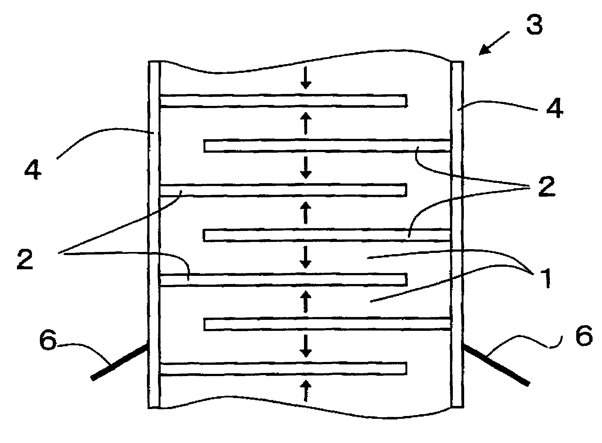
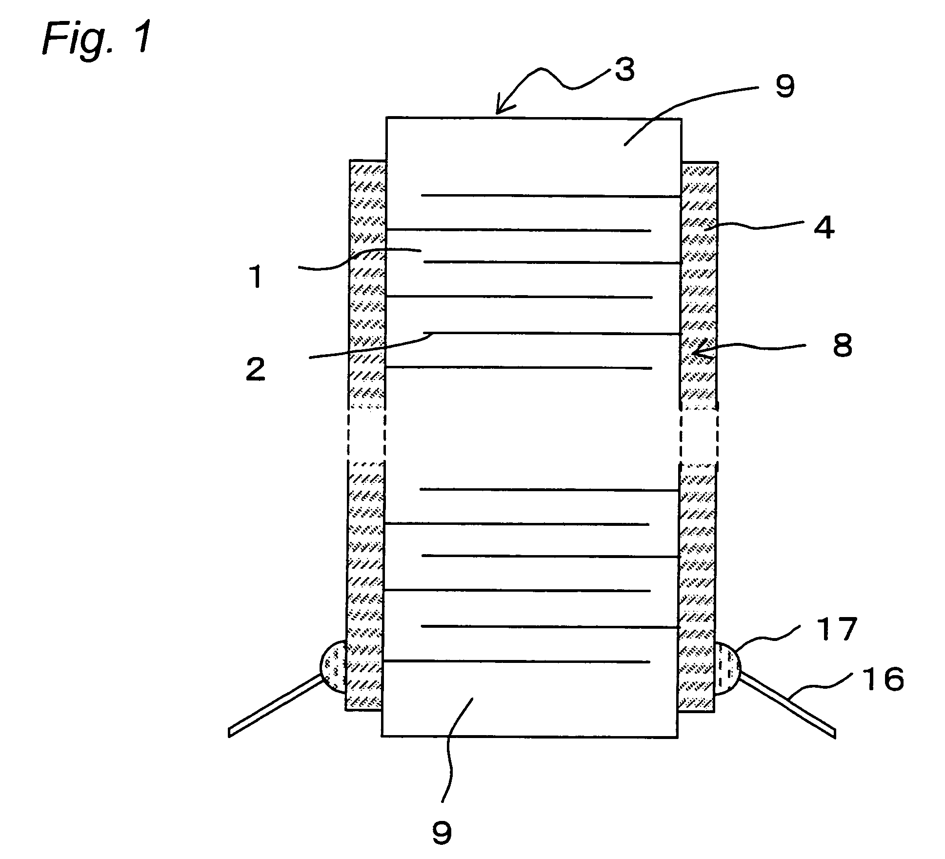
[0057]The multi-layer electronic component of the first embodiment has a column-like stack 3 of a rectangular prism shape comprising an active section 8 formed by stacking a plurality of ceramic layers 1 and a plurality of internal electrodes 2 alternately one on another, and inactive sections 9 provided on both ends of the active section 8 in the direction of stacking, as shown in FIG. 1.

[0058]The ceramic layer 1 is made of a piezoelectric ceramic material of which main component is lead zirconate titanate Pb(Zr, Ti)O3 (hereinafter abbreviated as PZT) or barium titanate BaTiO3, for example, but is not limited to this composition and may be made of any ceramic material that has piezoelectric property. The piezoelectric material preferably has a high value of piezoelectric strain co...

second embodiment

[0085]The multi-layer piezoelectric element according to the second embodiment of the present invention will be described in detail below.

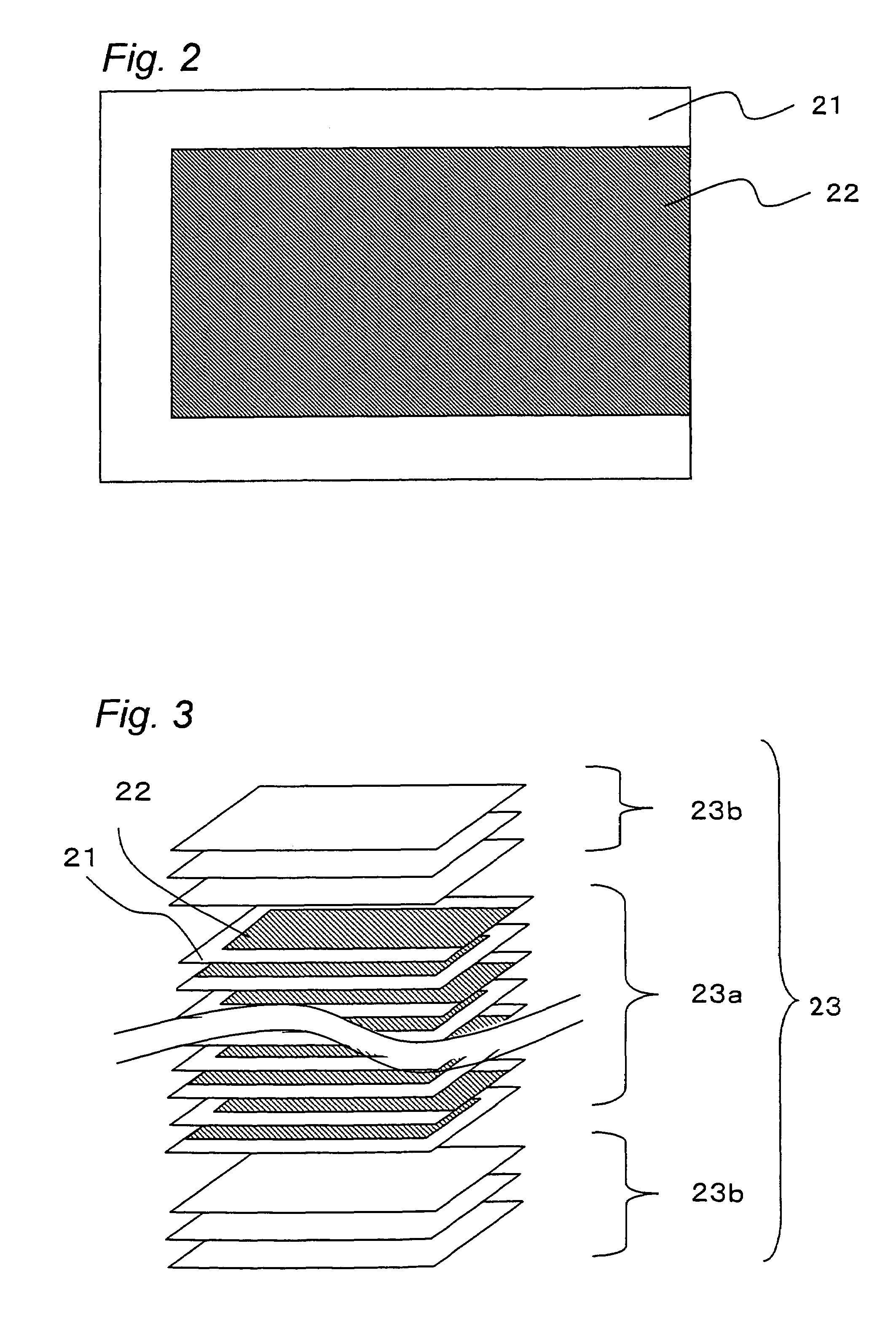
[0086]FIG. 6A is a perspective view showing the structure of a multi-layer piezoelectric element according to the second embodiment. FIG. 6B is an exploded perspective view of the inner structure of the multi-layer piezoelectric element according to the second embodiment, showing the stacked structure of the piezoelectric layers and the internal electrodes.

[0087]In the multi-layer piezoelectric element according to the second embodiment, as shown in FIG. 6A, B, external electrodes 15 are connected so as to establish electrical continuity with the ends of the internal electrodes 12 that are exposed in every other layer on a pair of opposing side faces of the stack 13 that is formed by alternately stacking the piezoelectric layers 11 and the internal electrodes 12 one on another. Layers on both ends in the stacking direction of the stack 13 are the ...

third embodiment

[0144]The piezoelectric electronic component according to the third embodiment of the present invention is a multi-layer piezoelectric actuator of similar constitution as that of the first embodiment, with a part of the manufacturing process different from that of the first embodiment.

[0145]FIG. 9 is an enlarged sectional view of a part of the multi-layer piezoelectric actuator of the third embodiment, with similar components identified with similar reference numerals as in the first embodiment.

[0146]Thickness of the piezoelectric layer 1, namely the distance between the internal electrodes 2, is preferably not larger than 200 μm, or more preferably not larger than 150 μm, in order to make the construction smaller and apply high electric field. On the other hand, thickness of the piezoelectric layer 1 is set not smaller than 50 μm, preferably not smaller than 70 μm, in order to reduce the transient time of applying a voltage to the piezoelectric layer 1 and enable faster response. T...


PUM


Abstract

In order to provide a multi-layer electronic component in which the occurrence of delamination between the ceramic layer and the internal electrode is restricted and a method for manufacturing the same, the multi-layer electronic component of the present invention comprises a stack formed by stacking piezoelectric layers and internal electrodes one on another alternately and a pair of external electrodes formed on two opposing side faces of the stack, wherein the internal electrode consists of a first internal electrode connected to the external electrode formed on one of the two side faces and a second internal electrode located between the first internal electrode and connected to the external electrode formed on the other one of the two side faces, and wherein the internal electrodes and the piezoelectric layers are faced in proximity so that a space between them is 2 μm or less over an area occupying 50% or more of the active region where the first internal electrode and the second internal electrode oppose each other.

Description

TECHNICAL FIELD[0001]The present invention relates to a multi-layer electronic component and a method for manufacturing the same, and particularly to a multi-layer piezoelectric element and an injection apparatus constituted by using the element. More particularly, the present invention relates to a multi-layer piezoelectric element used for fuel injection apparatus of automobile engine, liquid ejecting apparatus of ink jet printer or the like or a drive unit used in precision positioning device or vibration preventing device for an optical apparatus, or to a multi-layer piezoelectric element used as a sensor element mounted in combustion pressure sensor, knocking sensor, acceleration sensor, load sensor, ultrasonic sensor, pressure sensor, yaw rate sensor or the like, or used as a circuit component mounted in piezoelectric gyro, piezoelectric switch, piezoelectric transformer, piezoelectric breaker or the like.BACKGROUND ART[0002]Use of multi-layer piezoelectric element made by alt...

Claims


Application Information

Patent Timeline
Patent Type & Authority Patents(United States)
IPC IPC(8): H01L41/083H01L41/273
CPCH01L41/273H01L41/083H01L41/0471H10N30/871H10N30/50H10N30/053
Inventor ONO, SUSUMUOKAMURA, TAKESHISAKAUE, KATSUSHIHIRA, TAKAAKITERAZONO, MASAKI
Owner KYOCERA CORP
Why Eureka
Try Eureka