
Wide temperature range dielectric absorber

a dielectric absorber and temperature range technology, applied in the direction of electrical equipment, antennas, etc., can solve the problems of ineffective absorbing of electromagnetic radiation at that temperature, difficult to provide a dielectric absorber capable of uniformly absorbing electromagnetic radiation, and low net magnetization of ferromagnetic material

Active Publication Date: 2009-12-15
ALLUMAX TTI LLC
View PDF11 Cites 3 Cited by
  • Summary
  • Abstract
  • Description
  • Claims
  • Application Information

AI Technical Summary

Benefits of technology

[0008]A wide temperature range dielectric absorber, substantially as shown in and / or described in connection with at least one of the figures, and as set forth more completely in the claims.

Problems solved by technology

However, a ferromagnetic material loses its characteristic ferromagnetic ability at temperatures above the Curie temperature for that material, causing the net magnetization of the ferromagnetic material to be zero.
In applications subjected to a broad temperature range including very high temperatures, such as up to 1100° C., it has proven very difficult to provide a dielectric absorber capable of uniformly absorbing electromagnetic radiation.
However, many components of an aircraft can reach temperatures in excess of the effective electromagnetic absorption temperature, causing the absorber coating to be ineffective at absorbing electromagnetic radiation at that temperature.
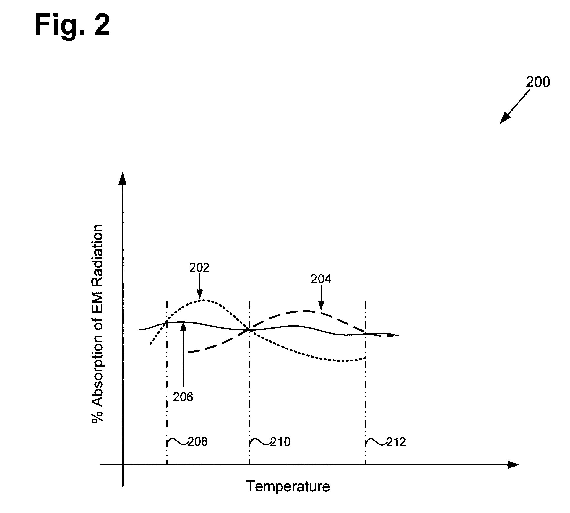
Furthermore, in applications subjected to a very broad temperature range, a single material dielectric absorber is ineffective at providing uniform electromagnetic radiation absorption over the entire temperature range.

Method used


Image

  • Wide temperature range dielectric absorber
  • Wide temperature range dielectric absorber
  • Wide temperature range dielectric absorber

Examples


Embodiment Construction

[0011]The present invention is directed to a wide temperature range dielectric absorber. Although the invention is described with respect to specific embodiments, the principles of the invention, as defined by the claims appended herein, can obviously be applied beyond the specifically described embodiments of the invention described herein. Moreover, in the description of the present invention, certain details have been left out in order to not obscure the inventive aspects of the invention. The details left out are within the knowledge of a person of ordinary skill in the art.

[0012]The drawings in the present application and their accompanying detailed description are directed to merely exemplary embodiments of the invention. To maintain brevity, other embodiments of the invention which use the principles of the present invention are not specifically described in the present application and are not specifically illustrated by the present drawings.

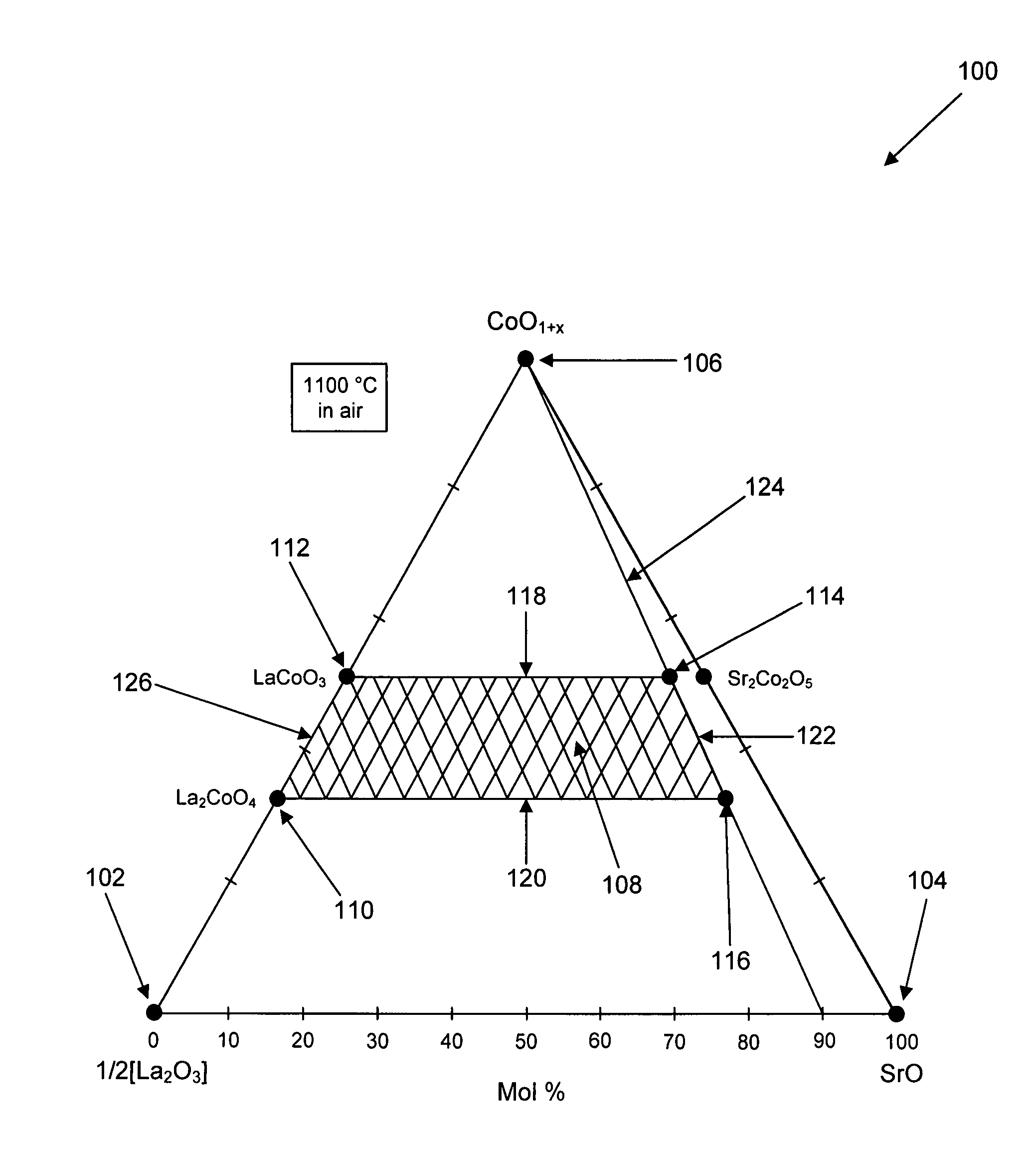
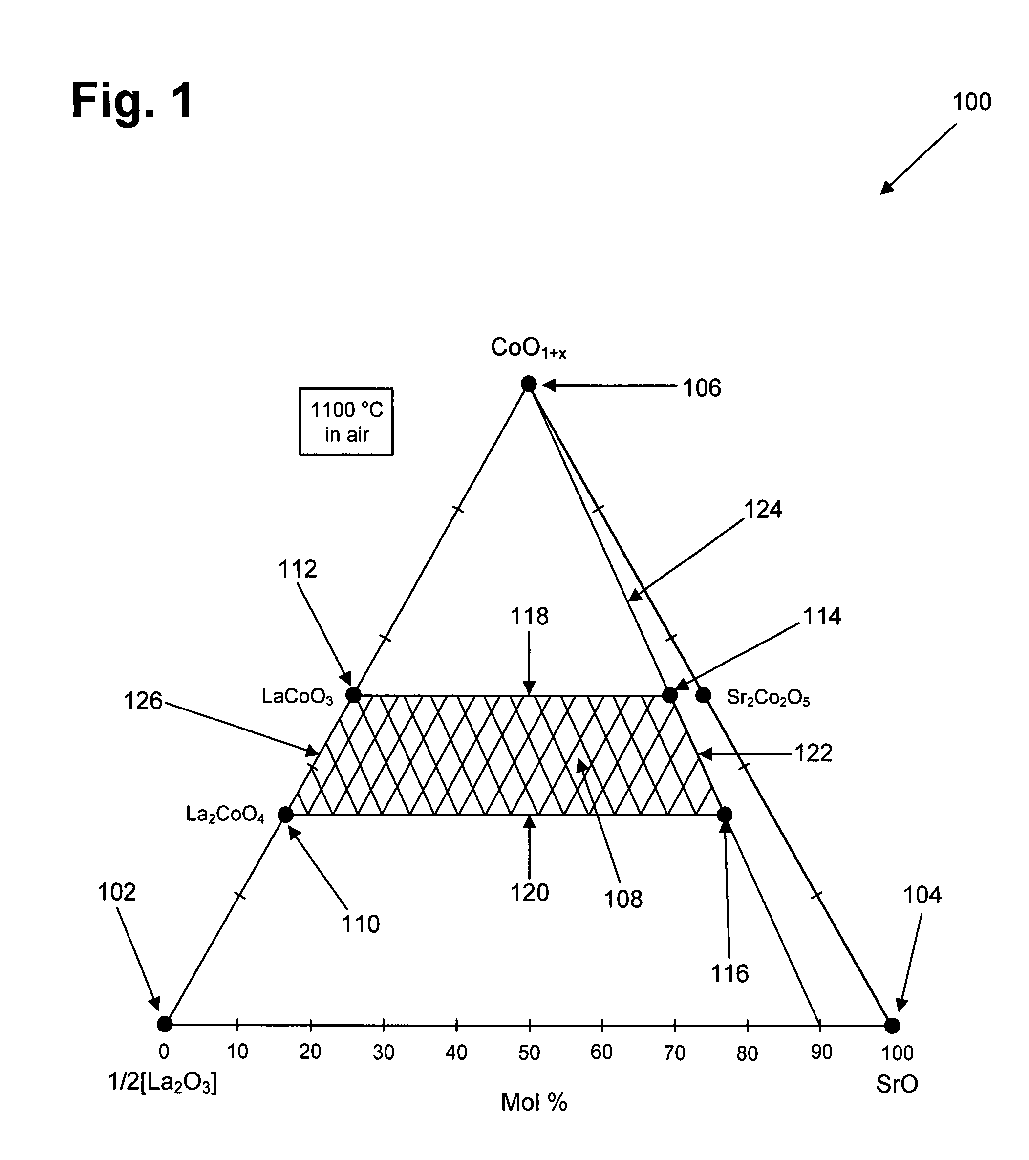
[0013]FIG. 1 represents ternary ph...


PUM

PropertyMeasurementUnit
temperatureaaaaaaaaaa
temperaturesaaaaaaaaaa

Abstract

According to one exemplary embodiment, a wide temperature range dielectric absorber includes a dielectric absorber comprising a blend of lanthanum oxide, strontium oxide, and cobalt oxide, and is represented by (1−z)[La1−xSrxCoO3±y]+z[La2−xSrxCoO4±y]. The dielectric absorber includes a first crystalline structure existing independently from a second crystalline structure causing the dielectric absorption composition to have a wide temperature range of electromagnetic radiation absorption. In one embodiment, the first crystalline structure is a perovskite crystalline structure and the second crystalline structure is a potassium nickel fluoride crystalline structure.

Description

[0001]The present application claims the benefit of and priority to a pending provisional patent application entitled “High Temperature Dielectric Absorber,” Ser. No. 60 / 811,919 filed on Jun. 8, 2006. The disclosure in that pending provisional application is hereby incorporated fully by reference into the present application.BACKGROUND OF THE INVENTION[0002]1. Field of the Invention[0003]The present invention relates to the field of dielectric absorbers. More specifically, the invention relates to dielectric absorbers of electromagnetic radiation.[0004]2. Background Art[0005]In many applications, such as aviation applications, it can be desirable for a structure to be “invisible” to or undetectable. For example, aircraft invisible to electromagnetic radiation is less likely to be spotted on a radar system, which can be desirable in some applications. Conventional approaches have utilized oxide or dielectric absorbent coatings comprising ferromagnetic materials to reduce reflection o...

Claims


Application Information

Patent Timeline
Patent Type & Authority Patents(United States)
IPC IPC(8): H01Q17/00
CPCC04B35/01H01Q17/00C04B2235/3213C04B2235/3275C04B2235/768C04B2235/3227
Inventor HILL, MICHAEL D.
Owner ALLUMAX TTI LLC
Learn More