Functional layer having wiring connected to electrode and barrier metal between electrode and wiring

a technology of functional layer and wiring, which is applied in the direction of ceramic layered products, discharge tube luminescent screens, transportation and packaging, etc., can solve the problem of increasing the light quantity loss due to optical reflection, inability to allocate sufficient large area to light-receiving portions, and existing imaging devices with several tens of percentages of light quantity loss, etc. problems, to achieve the effect of improving performance, good operation durability characteristics, and satisfactory performan

Inactive Publication Date: 2010-01-05
FUJIFILM HLDG CORP +1
View PDF15 Cites 11 Cited by
  • Summary
  • Abstract
  • Description
  • Claims
  • Application Information

AI Technical Summary

Benefits of technology

[0012]The present invention has been made in view of the circumstances mentioned above, and aims to provide a functional device having very good operation durability characteristics and ensuring high reliability and satisfactory performance even in fine patterning.
[0014]By having this structure, it becomes possible to prevent a contact failure caused by migration of metal contained in the electrodes or the wiring into adjacent layers, and operation durability characteristics can be improved.
[0025]By designing as mentioned above, the functional layers are prevented from suffering damage in photolithographic processing included in the process of forming the barrier metal.
[0028]By designing as mentioned above, the imaging device using such a functional device can have improved performances.
[0030]By designing as mentioned above, the display device using such a functional device can have improved performances.
[0031]According to the invention, it is possible to provide a functional device having very good operation durability characteristics and satisfactory performances.

Problems solved by technology

So there is a problem that a sufficiently large area cannot be allocated to the light-receiving portions.
However, such a measure has inevitable problems including an increase in light quantity loss due to optical reflection, so it is said that the existing imaging devices have several tens of percentages of light quantity loss.
In addition, the fineness requirements for solid-state imaging devices are becoming severer from year to year, and progress toward fining light-receiving portions leads to a problem that an incident light angle differential between the periphery and the center of an imaging device causes differences in light-gathering rates of microlenses to result in a shading phenomenon.
However, formation of functional devices by use of organic materials requires patterning electrodes on the functional layers, and fine patterning according to methods hitherto adopted suffers a problem that the devices formed deteriorate considerably in their performances.
In the case of photolithographic processing in particular, there is a problem that since a development process after exposure is essential therein, purified water used for washing treatment in the development process reaches an organic semiconductor layer and degrades the organic semiconductor layer; as a result, there occurs a marked drop in device performance.
However, when the migration as mentioned above occurs in the minimized contact regions, contact performance is lowered and device functionality is substantially reduced.
Although metal oxides such as ITO are in the mainstream of conductive materials widely used as light-pervious electrodes in photofunctional devices, such metal oxide-utilized devices have a problem that the immediate contact between metal oxide and aluminum traces causes reaction between the oxygen and the aluminum to result in considerable decrease of contact performance.

Method used


Image

  • Functional layer having wiring connected to electrode and barrier metal between electrode and wiring
  • Functional layer having wiring connected to electrode and barrier metal between electrode and wiring
  • Functional layer having wiring connected to electrode and barrier metal between electrode and wiring

Examples


first embodiment

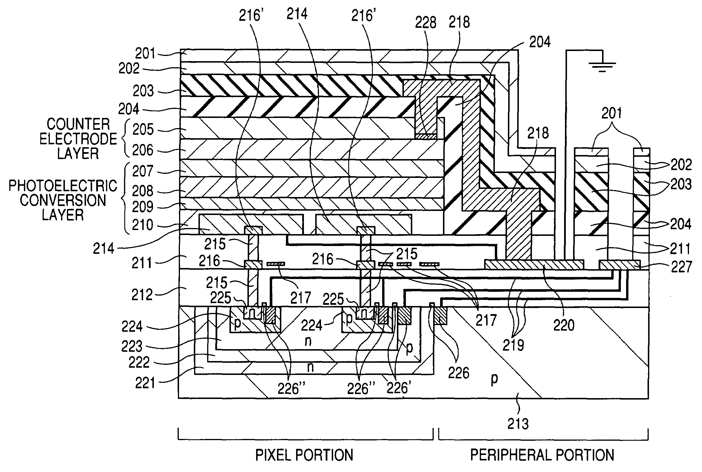
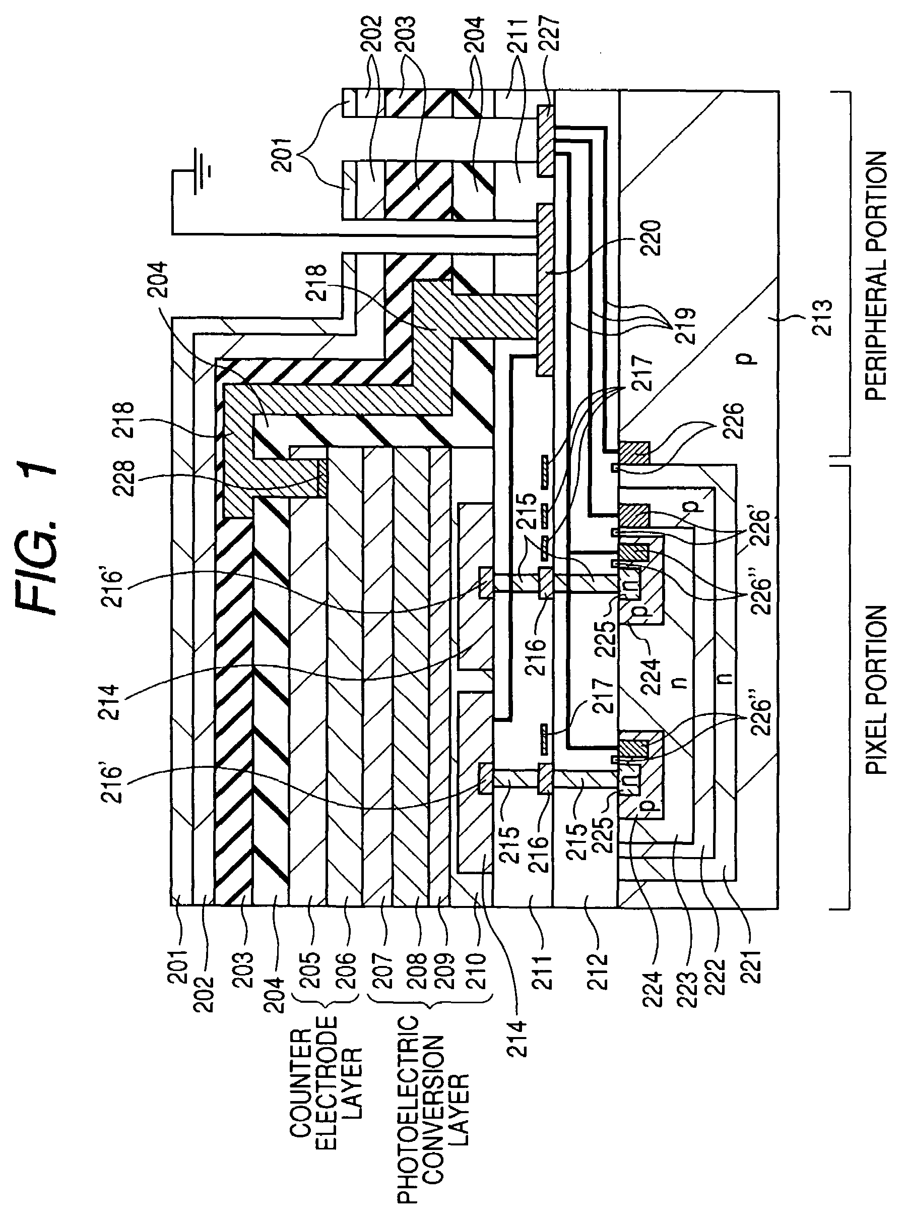
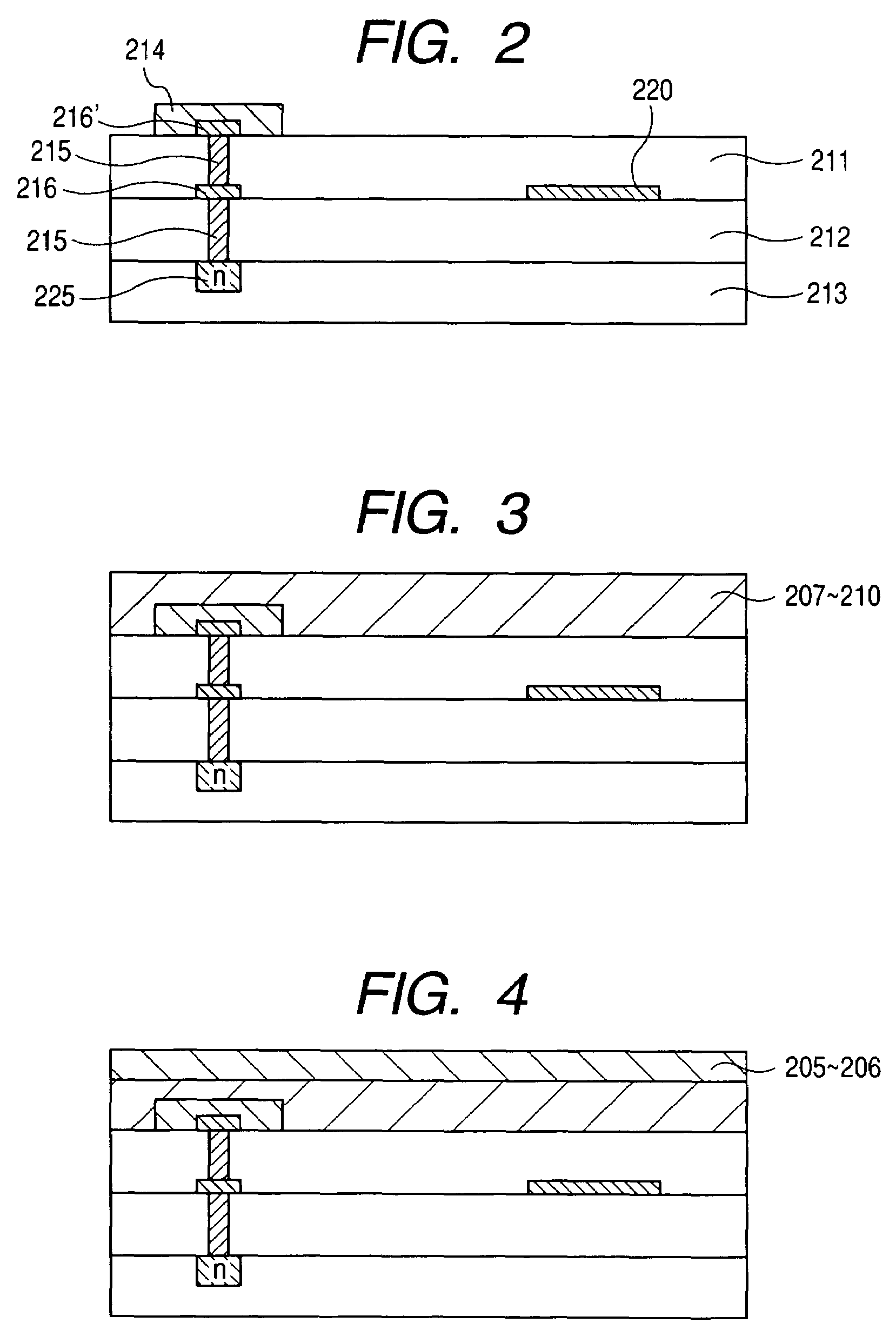
[0089]The photoelectric conversion layer-stacked solid-state imaging devices can have various structures, including a first structure which permits color imaging by depositing above a silicon substrate three photoelectric conversion layers, each of which is made up of two electrode layers and an organic material sandwiched between them, and detecting lights of three different colors above the silicon substrate and a second structure which is like as the structure shown in FIG. 5 of JP-A-2003-332551 and permits color imaging by depositing above a silicon substrate one photoelectric conversion layer made up of two electrode layers and an organic material sandwiched between them, forming two pn junctions inside the silicon substrate at positions differing in depth and detecting lights of two different colors inside the silicon substrate and light of another color above the silicon substrate. Taking the second structure as an example, a first embodiment of the invention is illustrated.

[...

second embodiment

[0130]In a second embodiment of the invention, the functional device has a structure that the second electrode layer is divided among pixels and a conductor trace is connected to each piece of the divided second electrode layer via barrier metal. Taking a luminescent device as an example, the second mode of functional device is illustrated below. The luminescent device is a device used in a display or the like. The following illustration is made taking the area emitting light for representing one pixel of an image as one pixel.

[0131]FIG. 13(a) is a schematic surface view showing a configuration outline of two pixels among those constituting the luminescent device, FIG. 13(b) is a schematic cross-sectional view taken on line α-α′ of FIG. 13(a), FIG. 13(c) is a diagrammatic drawing showing an example of a driving circuit of the luminescent device, and FIG. 13(d) is a diagrammatic drawing showing a traditional example of the driving circuit of a luminescent device. In FIG. 13(a), the c...

third embodiment

[0146]A third embodiment of the invention is illustrated with taking as an example of the structure of a photoelectric conversion layer-stacked solid-state imaging device the first structure that permits color imaging by depositing above a silicon substrate three photoelectric conversion layers, each of which is made up of two electrode layers and an organic material sandwiched between them, and detecting lights of three different colors above the silicon substrate.

[0147]FIG. 26 is a schematic surface view of a photoelectric conversion layer-stacked solid-state imaging device for illustrating the third embodiment of the invention. The photoelectric conversion layer-stacked solid-state imaging device 1100 shown in FIG. 26 has a great many light-receiving portions (pixels) 1101 arrayed in a grid pattern, or a matrix of pixels, in this example.

[0148]On the surface of a semiconductor substrate provided underneath the light-receiving portions 1101 in the photoelectric conversion layer-st...


PUM

PropertyMeasurementUnit
edge lengthaaaaaaaaaa
thicknessaaaaaaaaaa
thicknessaaaaaaaaaa

Abstract

A functional device having very good operation durability characteristics, high reliability and satisfactory performance is provided. The functional device provided is a functional device having: at least one functional layer deposited over a substrate wherein an organic material is included; and a plurality of electrodes for bringing the functional layer into action. And this functional device is provided with wiring connected to each of the plurality of electrodes and a barrier metal made to lie between at least one among the plurality of electrodes and the wiring connected thereto.

Description

[0001]This application is based on Japanese Patent application JP 2004-199825, filed Jul. 6, 2004, the entire content of which is hereby incorporated by reference. This claim for priority benefit is being filed concurrently with the filing of this application.BACKGROUND OF THE INVENTION[0002]1. Technical Field of the Invention[0003]The present invention relates to a functional device having a photoelectric conversion layer or a luminescent layer over a substrate in a deposited state.[0004]2. Description of the Related Art[0005]Functional devices using organic materials, notably organic luminescent devices, have made remarkable progress in recent years. And an organic EL display as a representative of organic luminescent devices has had a success in practical utilization. On the other hand, a photoelectric conversion device as an example of functional devices, though not yet successful in manufacturing, has made considerable strides in recent years, and has the potential to overcome ...

Claims


Application Information

Patent Timeline
Patent Type & Authority Patents(United States)
IPC IPC(8): H01J1/62H01J63/04
CPCH01L27/14632H01L27/14636H01L27/14687H01L31/102H01L27/14868Y10T428/24926Y10T428/24917
Inventor ARAKI, YASUSHI
Owner FUJIFILM HLDG CORP
Why Eureka
Try Eureka