Clocking of integrated circuits using photonics

a photonics and integrated circuit technology, applied in the field of communicating signals, can solve the problems of difficult if not impossible to achieve equal clocking, difficult to reduce or eliminate clock skew, and limited accuracy, and achieve the effect of facilitating oversampling of signals

Active Publication Date: 2010-01-12
ORACLE INT CORP
View PDF4 Cites 17 Cited by
  • Summary
  • Abstract
  • Description
  • Claims
  • Application Information

AI Technical Summary

Benefits of technology

[0025]In some embodiments, the second integrated circuit includes one or more receivers (such as a group of receivers) coupled to the optical clock path. Note that the optical signals facilitate oversampling of signals at the one or more receivers. For example, a given receiver in the group of receiver may be configured to be triggered using one or more of the optical signals. In some embodiments, the second integrated circuit includes a multiplexer between the optical clock path and the one or more receivers.

Problems solved by technology

Unfortunately, even with these circuit geometries, it is difficult if not impossible to achieve equal clocking because of effects such as clock skew and clock jitter.
This difference may be the result of a design error or a processing inaccuracy.
However, it is often difficult to reduce or eliminate clock skew 118 (FIG. 1) because mismatches between clock paths rarely arise until after a layout is completed and the performance of the design is extracted using simulations.
Unfortunately, the extraction process is complicated and has limited accuracy.
Unfortunately, aside from decreasing the overall insertion delay, further reducing or avoiding clock jitter 112 (FIG. 1) is difficult.
Furthermore, distributing clock signals also consumes power.
For example, distributing clock signals in existing high-performance microprocessors may consume up to 20% of the total chip power.
As clock frequencies continue to increase, this power consumption is becoming an increasing burden and is creating challenges for circuit designers.
These multi-phase clock signals are either generated at the receivers (at high area and power cost) or are distributed from a central clock source (with the associated clock skew and jitter problems discussed above).

Method used


Image

  • Clocking of integrated circuits using photonics
  • Clocking of integrated circuits using photonics
  • Clocking of integrated circuits using photonics

Examples


Embodiment Construction

[0048]The following description is presented to enable any person skilled in the art to make and use the invention, and is provided in the context of a particular application and its requirements. Various modifications to the disclosed embodiments will be readily apparent to those skilled in the art, and the general principles defined herein may be applied to other embodiments and applications without departing from the spirit and scope of the present invention. Thus, the present invention is not intended to be limited to the embodiments shown, but is to be accorded the widest scope consistent with the principles and features disclosed herein.

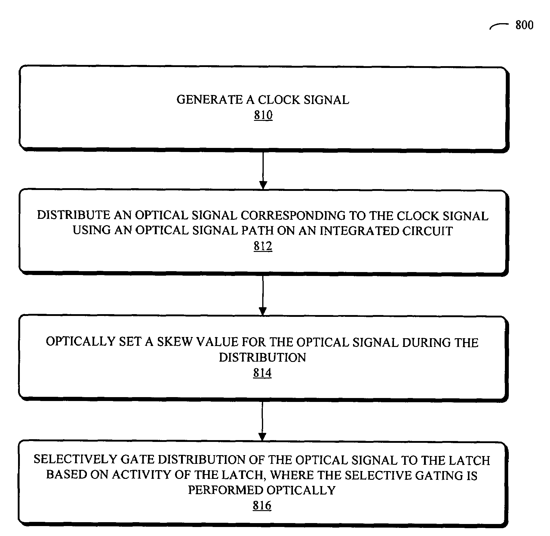
[0049]Embodiments of a method, a circuit, an integrated circuit, a semiconductor die that includes the integrated circuit, and a system that includes the semiconductor die are described. This integrated circuit is configured to distribute one or more clock signals to one or more circuits or components (such as an electronic latch and / or an opti...


PUM


Abstract

Embodiments of an integrated circuit are described. This integrated circuit includes: a clock-generator circuit configured to provide a clock signal; an optical clock path coupled to the clock-generator circuit; and a latch coupled to the optical clock path. This optical clock path is configured to distribute an optical signal corresponding to the clock signal. Furthermore, the optical clock path is configured to optically set a skew value for the optical signal, and is configured to selectively gate distribution of the optical signal to the latch based on activity of the latch. Note that the selective gating is performed optically.

Description

CROSS REFERENCE TO RELATED APPLICATIONS[0001]This application claims priority under 35 U.S.C. section 119(e) to U.S. Provisional Application Ser. No. 60 / 786,575, filed on Mar. 27, 2006, the contents of which are herein incorporated by reference.[0002]This application was filed by Park, Vaughan & Fleming LLP, 2820 Fifth Street, Davis, Calif. 95618, United States of America, (530) 759-1660.BACKGROUND[0003]1. Field of the Invention[0004]The present invention relates to techniques for communicating signals. More specifically, the present invention relates to using on-chip photonics to distribute and to adjust the skew or phase of clock signals.[0005]2. Related Art[0006]Many high-performance circuits or integrated circuits are clocked by a periodic clock signal to coordinate operations between circuit's elements. For example, a microprocessor may run at 2 GHz based on clock signals that have a clock period of 500 ps. In these circuits, it is often necessary to distribute the clock signal...

Claims


Application Information

Patent Timeline
Patent Type & Authority Patents(United States)
IPC IPC(8): H04B10/12
CPCG06F1/105
Inventor HO, RONALDCUNNINGHAM, JOHN E.KRISHNAMOORTHY, ASHOK V.DROST, ROBERT J.
Owner ORACLE INT CORP
Why Eureka
Try Eureka