Optical transceiver and method with channel binding, clock forwarding, and integrate-and-dump receivers

a transceiver and channel technology, applied in the field of optical networking systems and methods, can solve the problems of power and real estate waste, severe complicating process of further receiver bandwidth expansion, and inability to be easily satisfied, so as to simplify the clocking architecture and boost the sensitivity of the receiver

Active Publication Date: 2015-06-18
CIENA
View PDF11 Cites 13 Cited by
  • Summary
  • Abstract
  • Description
  • Claims
  • Application Information

AI Technical Summary

Benefits of technology

[0004]In various exemplary embodiments, an optical transceiver, method, and system optimize system design of WDM highly parallelized transceivers by binding optical channels, simplifying clocking architecture, and boosting receiver sensitivity. The optical transceiver, method, and system include clock recovery followed by data recovery and can utilize integrate-and-dump optical receivers with a recovered clock. In an exemplary embodiment, an optical transceiver includes N transmitters each transmitting N transmitted optically bound channels; a clock forwarding mechanism to transmit a transmitted optical clock signal to an opposing optical transceiver; N receivers each receiving one of N received optically bound channels; and a clock recovery mechanism to receive a received optical clock signal from the opposing optical transceiver. The optical transceiver can further include a multiplexer combining the N transmitted optically bound channels from the N transmitters; and a demultiplexer splitting N received optically bound channels to the N receivers. Optionally, the N transmitters, the clock forwarding mechanism, the N receivers, the clock recovery mechanism, the multiplexer, and the demultiplexer are photonically integrated. The optical transceiver can further include clock distribution and data recovery circuitry coupled to each of the N receivers and the clock recovery mechanism, wherein the clock distribution and data recovery circuitry is configured to recover the received optical clock prior to performing data recovery.
[0007]In another exemplary embodiment, a method includes transmitting a composite signal split into N optically bound channels and an optical clock signal associated with the N optically bound channels; receiving the N optically bound channels and the optical clock signal; recovering an optical clock from the optical clock signal; and performing data recovery of the N optically bound channels utilizing the optical clock signal. Optionally, the method further includes transmitting the optical clock signal over a designated clock carrying wavelength; and receiving the optical clock signal over the designated clock carrying wavelength with a clock receiver that is a low-power, low-complexity clock signal receiver relative to a data receiver for the N optically bound channels. Alternatively, the method further includes transmitting the optical clock signal superimposed as an external or internal small-index modulation of an overall intensity envelope of a whole bound channel; and receiving the optical clock signal by tapping a small amount of overall optical power and detecting the optical clock signal with a narrowband and highly sensitive clock photodetector. The method can further include transmitting the optical clock signal at a much lower sub-harmonic, compared to signal rate of the N optically bound channels. The method can further include receiving the N optically bound channels with N integrate-and-dump receivers. The method can further include utilizing an integration time of about 75% of a bit period providing sufficient time for sampling a value of integrated current and resetting an integrator by discharging an integrating capacitor during the remaining about 25% of the bit period.

Problems solved by technology

They are power and real estate wasteful due to massive parallel implementation of essentially redundant digital clock and data recovery (CDR) circuitry in every one of the individual channel receiver.
8, August 2010, severely complicating process of further receiver bandwidth expansion.
In view of imminent integration of photonic optical circuits and associated electronics, the power dissipation and real estate requirements for implementation of optical bound channels become of ultimate importance and cannot be easily satisfied within the architectural solutions inherent to conventional implementation of direct-detect WDM optical channels.

Method used


Image

  • Optical transceiver and method with channel binding, clock forwarding, and integrate-and-dump receivers
  • Optical transceiver and method with channel binding, clock forwarding, and integrate-and-dump receivers
  • Optical transceiver and method with channel binding, clock forwarding, and integrate-and-dump receivers

Examples


Embodiment Construction

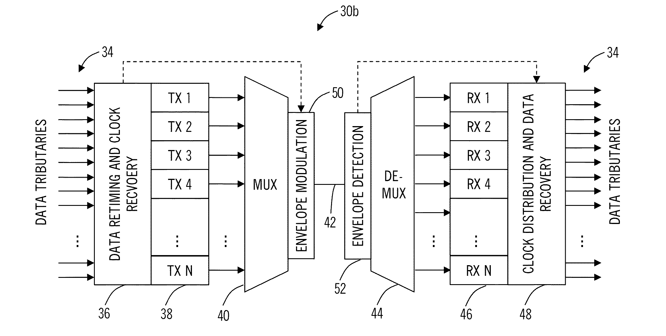
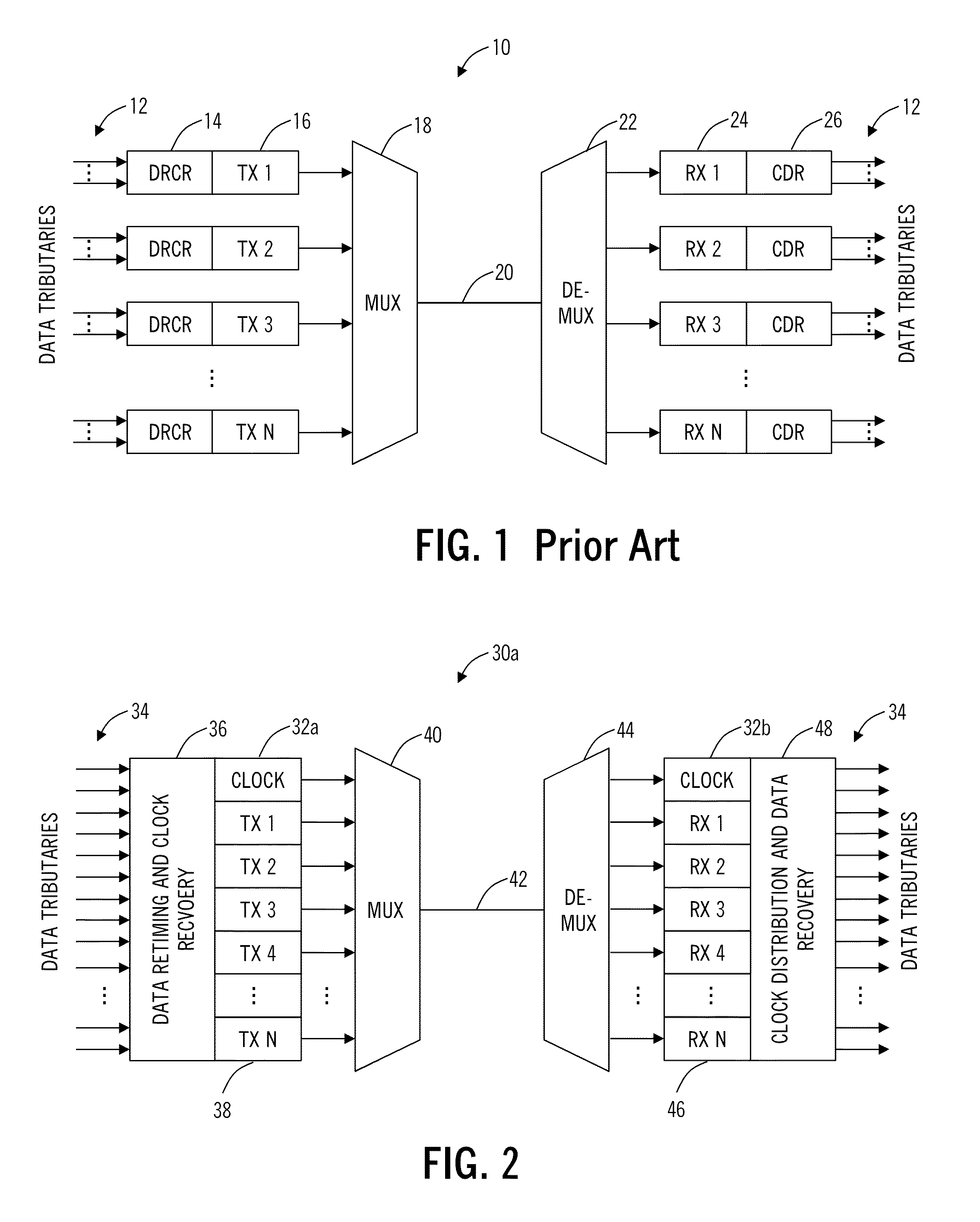
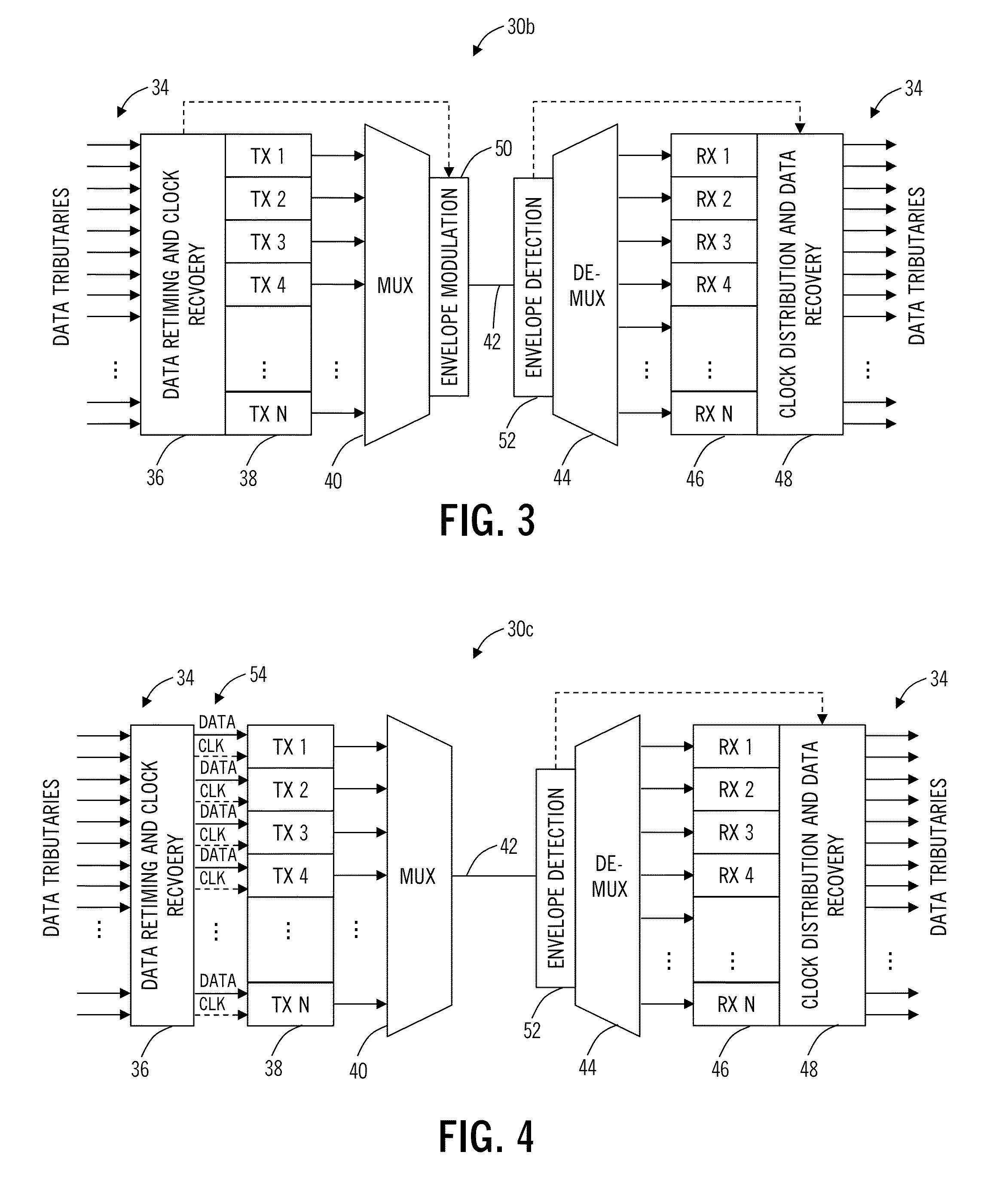
[0018]In various exemplary embodiments, an optical transceiver and method is disclosed to optimize system design of WDM highly parallelized transceivers by using optical bound channels, a simplified clocking architecture, and boosted receiver sensitivity. With application of photonic integration technology, highly parallelized transmitter and receiver arrays can be mass produced at low cost, making high-capacity point-point optical links much more feasible. Hence, simplified, efficient and cost effective WDM optical bound-channels disclosed herein can find wide usage in short reach chip-chip, board-board, data center, and metro-type applications. Optically bound channels include a signal X that is includes Y1, Y2, . . . , YN parts or segments that are each transmitted on a set of optical WDM carriers within the same optical module to create a composite line side signal where Y1+Y2+ . . . +YN=X. For example, optically bound channels can include 10×10 G, 4×25 G, etc. for a 100 G compo...


PUM


Abstract

An optical transceiver includes N transmitters each transmitting one of N transmitted optically bound channels; a clock forwarding mechanism to transmit a transmitted optical clock signal to an opposing optical receiver; N receivers each receiving one of N received optically bound channels; and a clock recovery mechanism to receive a received optical clock signal from the opposing optical transmitter. A method and photonically integrated system are also disclosed. The optical transceiver, method, and system optimize system design of WDM highly parallelized transceivers with optical bound channels, a simplified clocking architecture, and boosted receiver sensitivity. The optical transceiver, method, and system include clock recovery followed by data recovery and can utilize integrate-and-dump optical receivers with a recovered clock.

Description

FIELD OF THE DISCLOSURE[0001]The present disclosure relates generally to optical networking systems and methods. More particularly, the present disclosure relates to an optical transceiver and method with channel binding, clock forwarding, and integrate-and-dump receivers.BACKGROUND OF THE DISCLOSURE[0002]Optical links are finding increased use across a number of application spaces, including, for example, chip-chip, board-board, data center / rack-rack, in wide area network (WAN) fiber-optic links, and the like. All of these links and networks are experiencing rapidly increasing growth of capacity. WAN capacity growth is reflected by individual channel data rate scaling from 10 Gbps, to 40 Gbps, to currently deployed 100 Gbps, and to future projections of 1000 Gbps channels. The same capacity growth demand is also observed for shorter interconnects, as demonstrated by active optical cables which currently have >100 Gb of capacity (4×25 G, 10×10 G, etc.), and are starting to scale ...

Claims


Application Information

Patent Timeline
Patent Type & Authority Applications(United States)
IPC IPC(8): H04L7/00H04J14/02
CPCH04J14/02H04L7/0075H04J7/00H04J14/0226H04L7/0008H04J3/0685H04B10/40H04L25/14
Inventor PELEKHATY, VLADIMIRFRANKEL, MICHAEL Y.
Owner CIENA
Why Eureka
Try Eureka