Laser annealing apparatus for processing semiconductor devices in inline manner

a laser annealing and semiconductor technology, applied in the field of laser annealing apparatus, can solve the problems of increasing the possibility of damage to to-be-processed objects, complex manufacturing processes, drawbacks of conventional laser annealing apparatus, etc., and achieve the effect of fast and precise movemen

Active Publication Date: 2010-01-19
SAMSUNG DISPLAY CO LTD
View PDF7 Cites 27 Cited by
  • Summary
  • Abstract
  • Description
  • Claims
  • Application Information

AI Technical Summary

Benefits of technology

[0010]The present invention further provides a laser annealing apparatus, which can rapidly move a plurality of semiconductor devices subjected to an annealing process.
[0011]The present invention further provides a laser annealing apparatus, which can rapidly clean a plurality of semiconductor devices before and after an annealing process.
[0014]The plurality of first nozzles may be gas inlets, and the plurality of second nozzles may be gas outlets, such that gas introduced from one side can be easily discharged to the other side.
[0015]The moving unit may include movable stages, which temporarily carry thereon the to-be-processed objects, and a driving unit, which horizontally moves the movable stages. The driving unit may drive the movable stages when the laser beams are not emitted faster than when the laser beams are emitted, thereby allowing the semiconductor devices to be fast manufactured and improving productivity. For example, the moving unit may further comprise a transport speed adjusting photo-detector, which is vertically spaced apart from a horizontal trajectory of the plurality of to-be-processed objects and detects positions of the plurality of to-be-processed objects. The driving unit may change the transport speed of the movable stages according to whether the transport speed adjusting photo-detector detects light or not. For example, the moving unit may include first and second transport speed adjusting photo-detectors, and the driving unit may measure a time taken from when the first transport speed adjusting photo-detector detects the movable stages to when the second transport speed adjusting photo-detector detects the movable stages to calculate a current transport speed of the movable stages, and adjust the transport speed of the movable stages according to the calculation results.
[0017]Meanwhile, the apparatus may further include a cleaning unit, which is installed at a level with the laser beam emitting unit and the plurality of nozzles. Accordingly, the moving unit may move the plurality of to-be-processed objects during a laser annealing process at the same speed as the plurality of to-be-processed objects are moved during a cleaning process in the cleaning unit. In this manner, the to-be-processed objects, which have been cleaned before the laser annealing process, can be transported smoothly when the annealing process starts. Furthermore, the to-be-processed objects, which have been laser-annealed after the cleaning process, can be transported smoothly when the laser annealing process ends. In one embodiment, the moving unit may extend into the cleaning unit so that a separate moving unit for moving the plurality of to-be-processed objects need not be installed inside the cleaning unit. In this case, since delay time between the cleaning process in the cleaning unit and the laser annealing process is rarely needed, a fast and exact movement can be ensured.

Problems solved by technology

However, the general heat treatment has a problem in that a glass substrate used as a substrate of an OLED or an LCD is exposed to a high temperature atmosphere of 600° C. or more, and thus, the possibility of damage to to-be-processed objects increases.
The conventional laser annealing apparatus has a drawback, however, because just one semiconductor device can be manufactured using one annealing laser, and a cleaning process should be individually performed on each semiconductor device.
As a result, manufacturing processes are complex and rapid manufacture cannot be achieved.

Method used


Image

  • Laser annealing apparatus for processing semiconductor devices in inline manner
  • Laser annealing apparatus for processing semiconductor devices in inline manner
  • Laser annealing apparatus for processing semiconductor devices in inline manner

Examples


Embodiment Construction

[0027]The present invention will now be described more fully with reference to the accompanying drawings, in which preferred embodiments of the invention are shown.

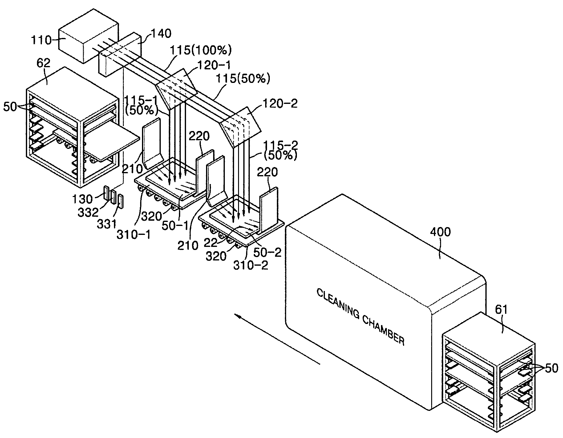
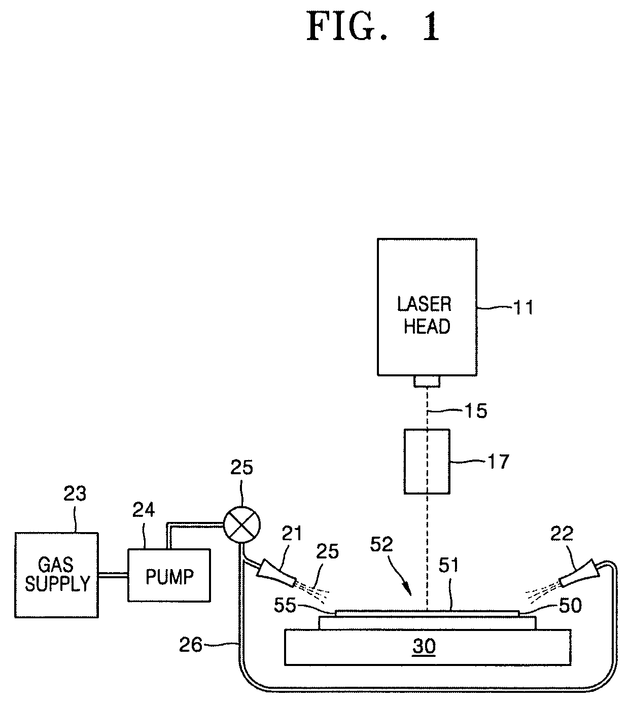
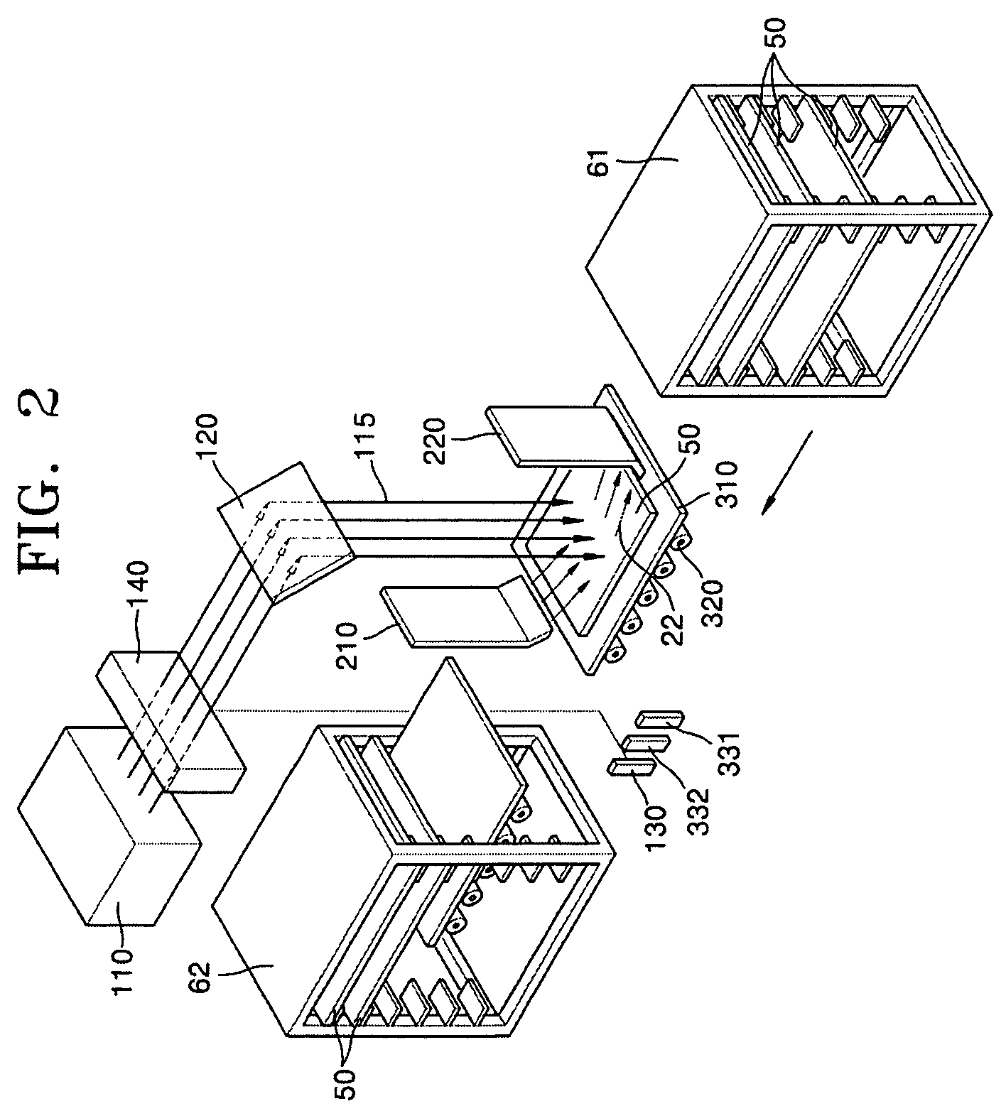
[0028]FIG. 2 is a perspective view illustrating an embodiment where a to-be-processed object 50 is processed while being moved in the laser annealing apparatus of FIG. 1. Referring to FIG. 2, to process objects in an open type chamber in an inline manner, gas, such as helium, neon, argon, nitrogen, etc., is introduced strongly through a nozzle 210, which is disposed on a left side of the to-be-processed object 50, and is exhausted strongly through a nozzle 220, which is disposed on a right side of the to-be-processed object 50. If there is no difficulty in forming an atmosphere suitable for a laser annealing process, both the left nozzle 210 and the right nozzle 220 can be gas inlets. A laser beam 115 having a predetermined power output from a laser head 110 is reflected by a reflector 120. The reflected laser beam 115 is...


PUM

PropertyMeasurementUnit
temperatureaaaaaaaaaa
reflectanceaaaaaaaaaa

Abstract

A laser annealing apparatus is provided, which can simultaneously process a plurality of moving semiconductor devices in an inline manner using one annealing laser. The apparatus may include a laser beam emitting unit, which emits laser beams to target regions of a to-be-processed object. Also included may be a plurality of first nozzles and a plurality of second nozzles, through which gas used for controlling an atmosphere of the target regions of the to-be-processed object is introduced or exhausted. The first and second nozzles may face each other so that the laser beams emitted from the laser beam emitting unit fall therebetween. The apparatus may further include a moving unit, which horizontally moves the to-be-processed object, to which the laser beams are emitted, at approximately the same transport speed.

Description

BACKGROUND OF THE INVENTION[0001]This application claims the priority of Korean Patent Application No. 2003-84899, filed on Nov. 27, 2003, in the Korean Intellectual Property Office, the disclosure of which is herein incorporated by reference in its entirety.FIELD OF THE INVENTION[0002]The present invention relates to a laser annealing apparatus for processing a plurality of semiconductor devices in an inline manner, and more particularly, to a laser annealing apparatus for processing a plurality of moving semiconductor devices in an inline manner using one annealing laser and a plurality of reflectors to manufacture highly reliable semiconductor devices rapidly with reduced manufacturing costs.DESCRIPTION OF THE RELATED ART[0003]An Amorphous Silicon Thin Film Transistor (a-Si TFT) has been used as a switching element of an Active Matrix-Organic Electro Luminescence Display (AM-OLED) or an Active Matrix-Liquid Crystal Display (AM-LCD). However, as demands for high quality displays c...

Claims


Application Information

Patent Timeline
Patent Type & Authority Patents(United States)
IPC IPC(8): B23K26/06H04N1/46H01L21/324
CPCH01L21/268H01L21/324
Inventor LEE, HONG-RO
Owner SAMSUNG DISPLAY CO LTD
Why Eureka
Try Eureka