Load calculating device and load calculating method

a technology of calculating device and load, which is applied in the direction of testing circuits, instruments, nuclear elements, etc., can solve the problems of thermal fatigue damage of solder junctions, damage to electronic circuit boards in electronic devices, and increased risk of failure of electronics circuit boards

Active Publication Date: 2010-01-26
KK TOSHIBA
View PDF7 Cites 21 Cited by
  • Summary
  • Abstract
  • Description
  • Claims
  • Application Information

AI Technical Summary

Problems solved by technology

An electronics circuit board in the electronic apparatus may thus be damaged depending on the design thereof.
Thus, the electronics circuit board may be at a higher risk for possible failures such as thermal fatigue damage to solder junctions, inappropriate insulation resulting from electromigration or whisker, element cracks, damage to micro-junctions, swelling or stripping of resin, and damage to wiring.
Further, users' various purposes of utilization of the electronics circuit board further increase the uncertainty of the estimation of loads, which is important in reliability design.
However, for digital information apparatuses, users have various purposes of utilization, so that in more and more cases, the conventional estimation conditions for the field load fail to correspond to reality.
The failure phenomenon estimation problem involves a tradeoff between a plurality of failure modes and is complicatedly associated with a large number of parameters.
It is thus difficult to determine how to deal with the problem only on the basis of local examinations.
For individual problems that have been sufficiently verified by failure phenomenon analysis, such an itemized design method often leads to high-performance processes owing to calibration data accumulated for many years.
Further, such quick, responsive guidelines are important in a chaotic time of foundation.
However, failure estimating methods or reliability designing methods overly adapted to the individual problems are often readily affected by a variation in circumstances or conditions.
Furthermore, such a method has difficulty dealing quickly with new problems, possibly reducing general efficiency.

Method used


Image

  • Load calculating device and load calculating method
  • Load calculating device and load calculating method
  • Load calculating device and load calculating method

Examples


Embodiment Construction

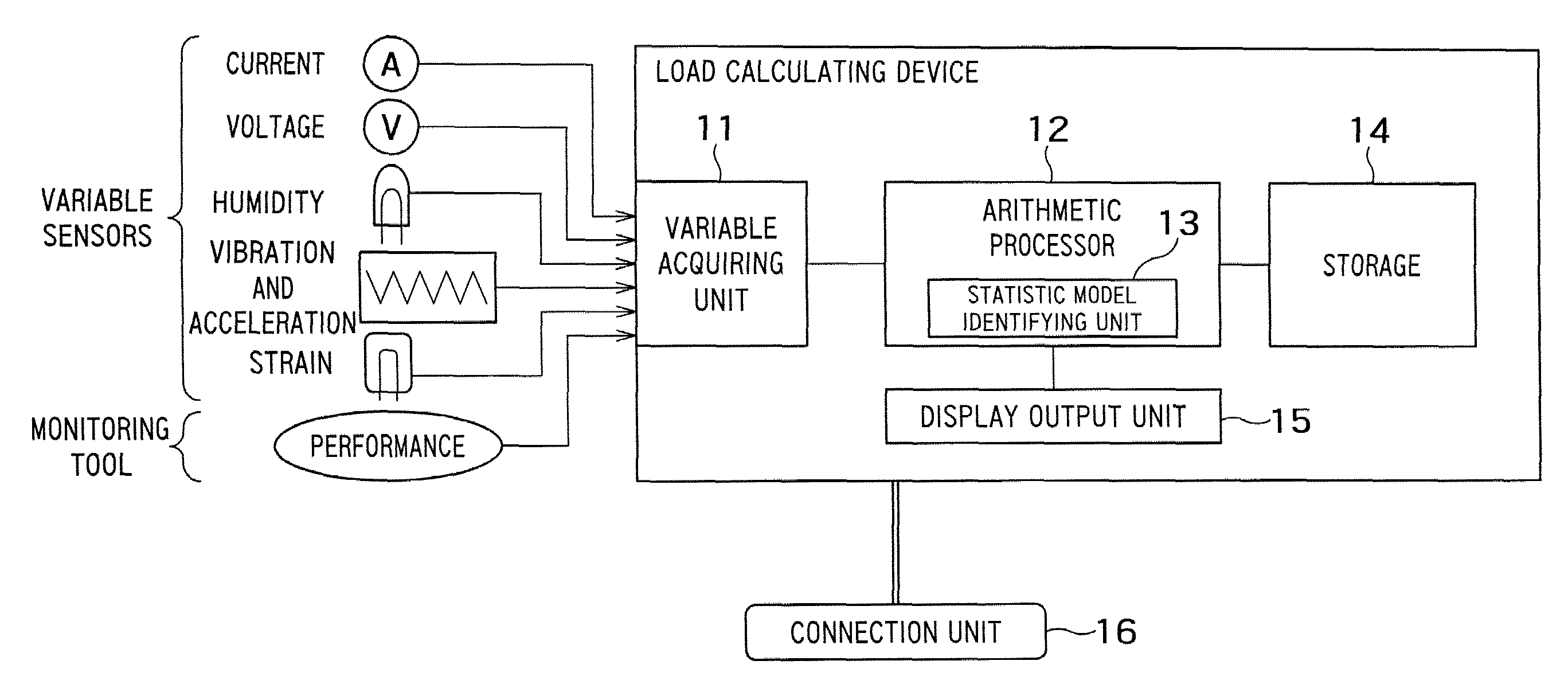
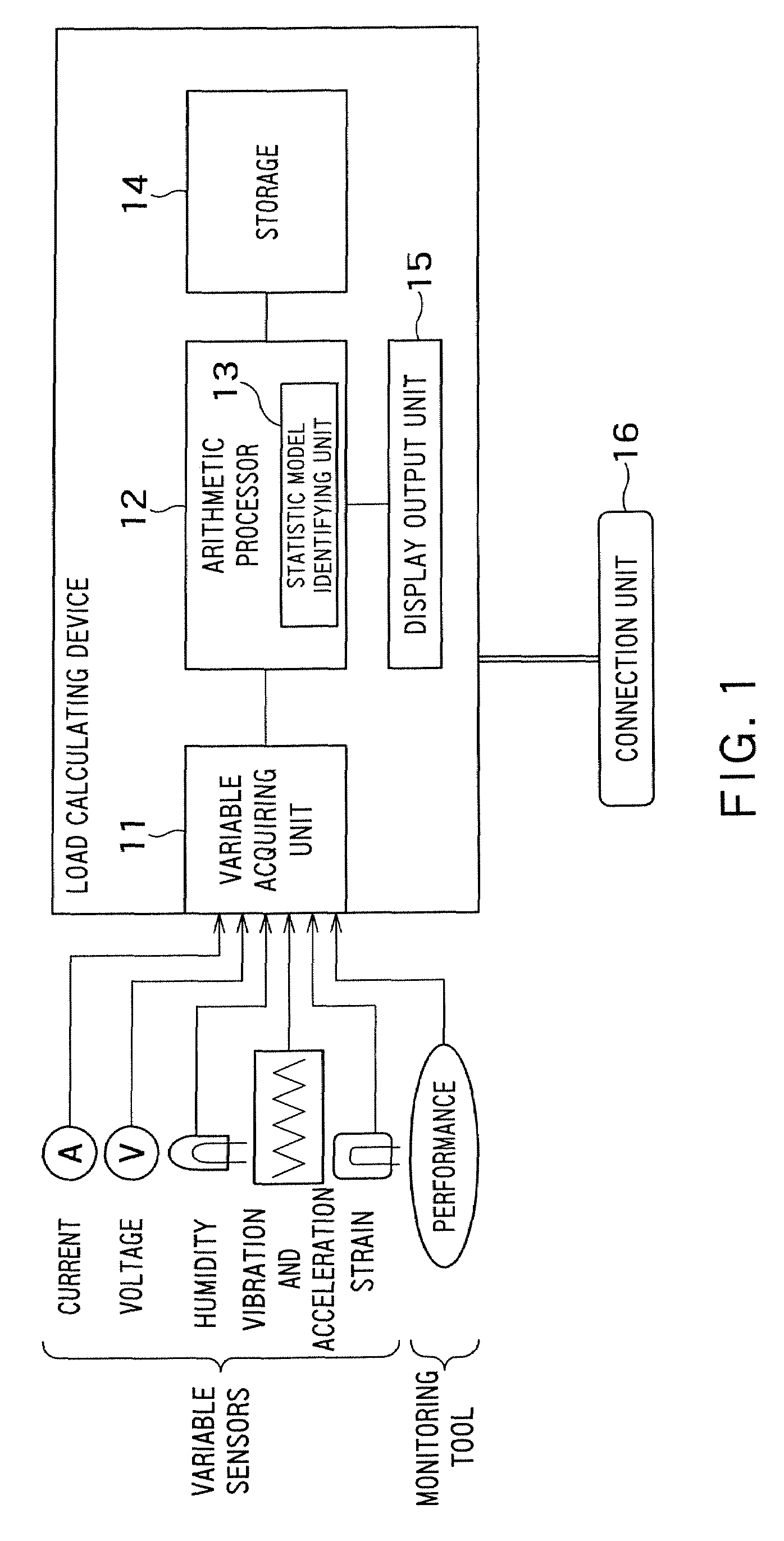
[0041]With reference to the drawings, description will be given of a load calculating device in accordance with an embodiment of the present invention. FIG. 1 shows the load calculating device in accordance with an embodiment of the present invention.

[0042]The load calculating device estimates a certain physical quantity (the time, space, and frequency distributions of the physical quantity) relating to a failure phenomenon for at least one place on an electronics circuit board built into an electronic apparatus such as a notebook personal computer. The load calculating device further determines the occurrence probability distribution of a failure mode (for example, a heat dissipation degradation occurrence probability distribution, a junction fatigue occurrence probability distribution, or an inappropriate insulation occurrence probability distribution) on the basis of the estimated distribution of the physical quantity or predicts the life expectancy distribution of the electronic...


PUM


Abstract

A device and method for providing a load calculating device is presented. In one embodiment, a load calculating device can include a variable acquiring unit configured to acquire monitoring variables. The monitoring variables can include in a detected value by a sensor monitoring a state of a circuit board and a performance characteristic obtained by a tool monitoring performance of the circuit board. The device can also store a first statistical model that is one of a regression model, an occurrence frequency distribution and a probability distribution; a second storage configured to store a second statistical model that is one of a regression model, an occurrence frequency distribution and a probability distribution. An arithmetic processor can then be used to calculate the intermediate variable from the monitoring variables according to the first statistical model and calculate the physical quantity from calculated intermediate variable according to the second statistical model.

Description

CROSS REFERENCE TO RELATED APPLICATIONS[0001]This application is based upon and claims the benefit of priority from the prior Japanese Patent Applications No. 2007-81687, filed on Mar. 27, 2007; the entire contents of which are incorporated herein by reference.BACKGROUND OF THE INVENTION[0002]1. Field of the Invention[0003]The present invention relates to a load calculating device and a load calculating method which estimate a physical quantity relating to a failure phenomenon at least one place on an circuit board located in an electronic apparatus while the electronic apparatus is in operation, to execute a load calculation or fault diagnosis on the circuit board on the basis of the estimated physical quantity.[0004]2. Related Art[0005]Electronic apparatuses may be subjected to loads resulting from physical or chemical effects associated with a manufacture, test, or use environment. An electronics circuit board in the electronic apparatus may thus be damaged depending on the desig...

Claims


Application Information

Patent Timeline
Patent Type & Authority Patents(United States)
IPC IPC(8): G06F17/18
CPCG01R31/2803
Inventor HIROHATA, KENJIMUKAI, MINORUHISANO, KATSUMIKAWAKAMI, TAKASHI
Owner KK TOSHIBA
Why Eureka
Try Eureka