Flicker reduction method, image pickup device, and flicker reduction circuit

a flicker reduction and flicker reduction technology, applied in the field of flicker reduction methods, image pickup devices, flicker reduction circuits, can solve the problems of substantially degrading image quality, reducing the free amount adjustment means for obtaining an appropriate amount of exposure, and unable to suppress flickering, etc., to achieve high precision, easy estimation, and high precision

Active Publication Date: 2010-02-02
SONY CORP
View PDF10 Cites 25 Cited by
  • Summary
  • Abstract
  • Description
  • Claims
  • Application Information

AI Technical Summary

Benefits of technology

[0051]In accordance with the flicker reduction method of the present invention, a signal component other than a flicker component is removed as the normalized integrated value or the normalized difference value, and a signal that allows the flicker component to be easily estimated at a high precision is obtained from a black background portion and a low-illuminance portion, each portion having a small amount of flicker component. By extracting the spectrum to an appropriate order from the normalized integrated value and the normalized difference value, the flicker component is thus estimated at a high precision regardless of the type of a fluorescent lamp and a luminance varied waveform even in an area where a signal component becomes discontinuous by the effect of a subject. The flicker component is reliably and sufficiently reduced from the input image signal by performing the calculation operation on the estimated flicker component and the input image signal.
[0052]In particular, in accordance with the flicker component reduction method of the second or third invention, the flicker component is detected from the color signal of each color, obtained as the video signal, on a per color signal basis, or on a per luminance and color signal basis, and the detected flicker component is reduced. The fluorescent light flicker containing the color flicker is thus accurately detected and reliably and sufficiently reduced.

Problems solved by technology

However, since this method does not allow the exposure time to be set to any value, the freedom of the exposure amount adjustment means for obtaining an appropriate amount of exposure is reduced.
Since all pixels are different in the exposure timing, the above-referenced method cannot suppress the flickering.
In practice, however, the above-described color variation also additionally appears, thereby substantially degrading image quality.
The XY addressing type scanning image pickup device suffers more from image quality degradation because the effect of the color flicker also appears on the screen.
With a variable electronic shutter speed feature incorporated, a CMOS image pickup device becomes complex in structure.
As disclosed in patent documents 1 and 2, the technique of estimating of the flicker component by measuring the amount of light of the fluorescent lamp with the photosensitive element or the measuring element increases the size and the cost of the image pickup system because the photosensitive element or the measuring element is attached to the image pickup device.
As disclosed in patent document 3, the technique of estimating the flicker component by photographing the two types of images in the different shutter conditions (exposure conditions) requires a complex system in the image pickup device, and further this technique is not appropriate for taking a moving image.
It is practically impossible to prepare the correction coefficients for all types of fluorescent lamps.
Depending on the type of the fluorescent lamp, detecting accurately the flicker component and reducing reliably the flicker component are difficult.
As the technique disclosed in patent document 3, the technique disclosed in patent document 5 for estimating the flicker component by photographing the two types of images at the different timings requires a complex system in the image pickup device and is not appropriate for taking a moving image.

Method used


Image

  • Flicker reduction method, image pickup device, and flicker reduction circuit
  • Flicker reduction method, image pickup device, and flicker reduction circuit
  • Flicker reduction method, image pickup device, and flicker reduction circuit

Examples


Embodiment Construction

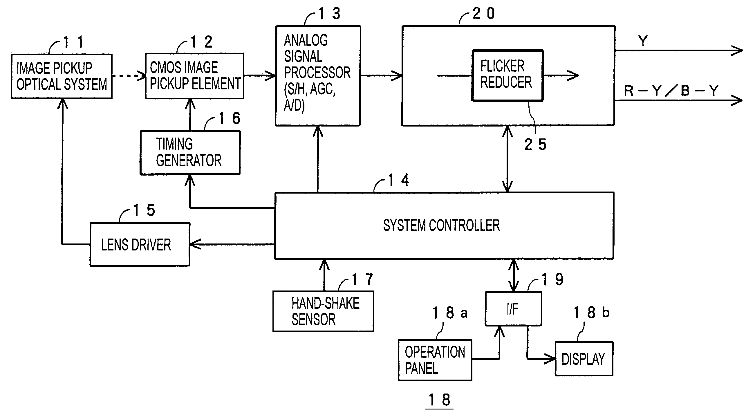
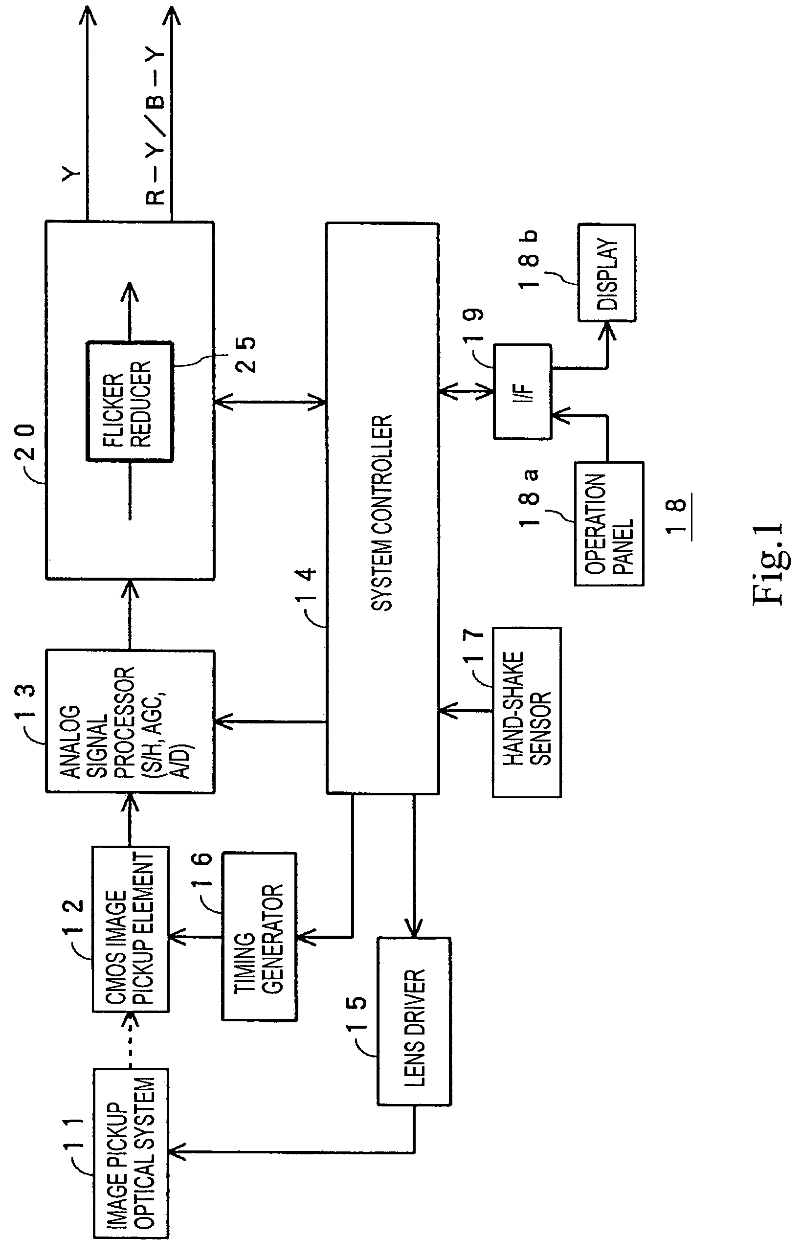
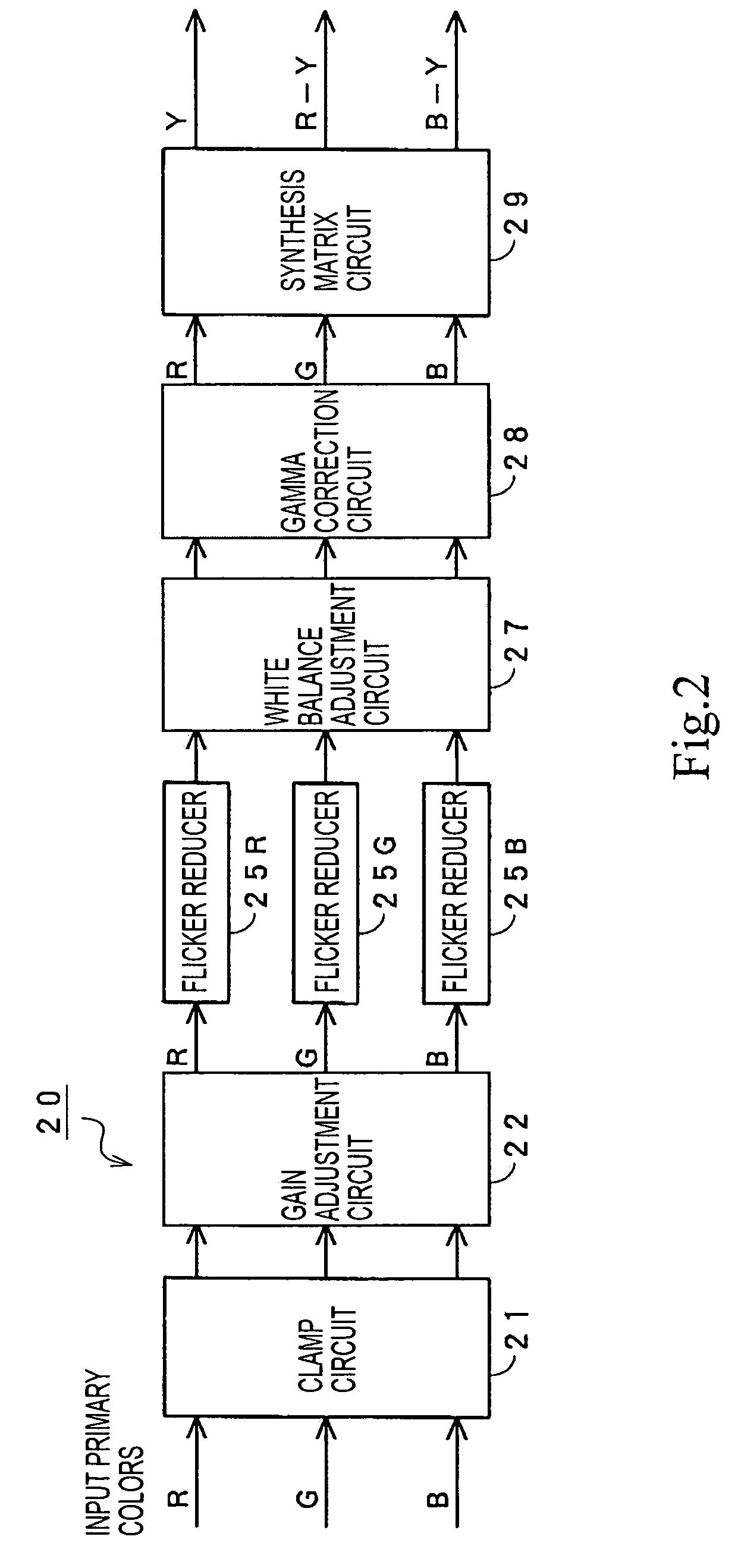
[0084][Embodiments of Image Pickup Devices: FIG. 1-FIG. 3]

[0085](System Configuration: FIG. 1)

[0086]FIG. 1 illustrates a system configuration of one embodiment of an image pickup device in accordance with the present invention. The image pickup device is here a video camera employing a CMOS image pickup element as a XY addressing type scanning image pickup -element.

[0087]In the image pickup device of this embodiment, namely, the video camera, light from a subject is incident on a CMOS image pickup device 12 via an image pickup optical system 11, and photoelectrically converted into an analog video signal by the CMOS image pickup device 12. The resulting analog video signal is thus obtained from the CMOS image pickup device 12.

[0088]The CMOS image pickup device 12 includes, on a CMOS substrate, a plurality of two-dimensionally arranged pixels, each pixel including a photodiode (a photo gate), a transfer gate (shutter transistor), a switching transistor (address transistor), an amplif...


PUM


Abstract

A system and method in which a fluorescent light flicker characteristic of an XY addressing type image pickup device such as a CMOS image pickup device is accurately detected and reliably and sufficiently reduced. This is achieved through signal processing without using a photosensitive element regardless of the level of a video signal of a subject and the type of a fluorescent lamp. A signal In′(x,y) is an RGB primary color signal or a luminance signal, each containing a flicker component. The signal In′(x,y) is integrated over a duration of time equal to or longer than one horizontal period, and a difference value between the integrated values of adjacent fields is normalized by the average value of the integrated values of three consecutive fields.

Description

TECHNICAL FIELD[0001]The present invention relates to a method for reducing a fluorescent light flicker occurring in a video signal from an XY addressing type scanning image pickup element (an imager or an image sensor) such as a CMOS (complementary metal oxide semiconductor) image pickup element when a subject is photographed by the image pickup element under light of a fluorescent lamp, an image pickup device, such as a video camera or a digital still camera employing the XY addressing type scanning image pickup element such as the CMOS image pickup element, and a flicker reduction circuit for use in the image pickup device.BACKGROUND ART[0002]When a subject is photographed by a video camera under an illumination of a fluorescent lamp directly operated from commercial AC power, chronological brightness level variations in a video signal as an image output, i.e., a fluorescent light flicker occurs due to a difference between the frequency (twice the frequency of the commercial AC p...

Claims


Application Information

Patent Timeline
Patent Type & Authority Patents(United States)
IPC IPC(8): H04N9/73H04N5/228G06T5/00H04N5/235H04N5/243H04N5/335H04N5/351H04N5/353H04N5/357H04N5/374H04N5/378H04N9/04
CPCH04N5/2357H04N5/243H04N23/745H04N23/76H04N25/60
Inventor KINOSHITA, MASAYANAKAMURA, MAKIBITANAKA, KENJI
Owner SONY CORP
Why Eureka
Try Eureka