Shift register and image display apparatus containing the same
a technology of image display apparatus and shift register, which is applied in the field of shift register to achieve the effect of improving driving reliability and increasing circuit area
- Summary
- Abstract
- Description
- Claims
- Application Information
AI Technical Summary
Benefits of technology
Problems solved by technology
Method used
Image
Examples
first preferred embodiment
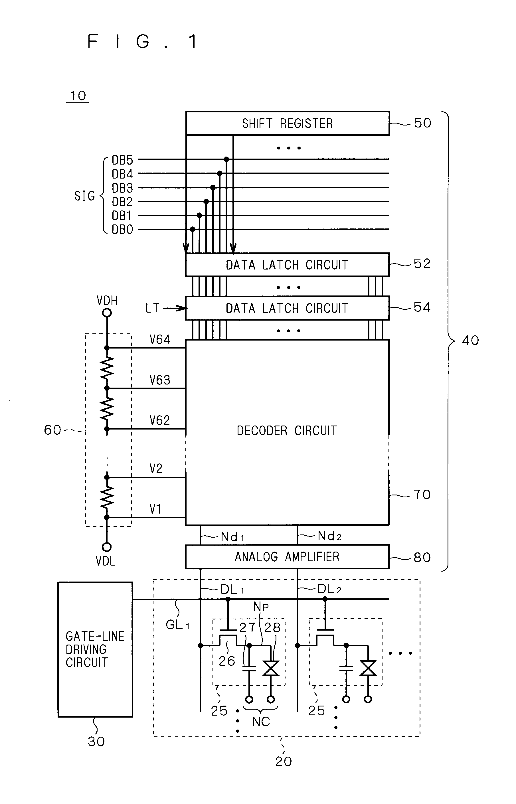
[0057]FIG. 1 is a schematic block diagram illustrating the configuration of a display apparatus according to the present invention. The overall configuration of a liquid crystal display 10 is shown as an representative example of the display apparatus.
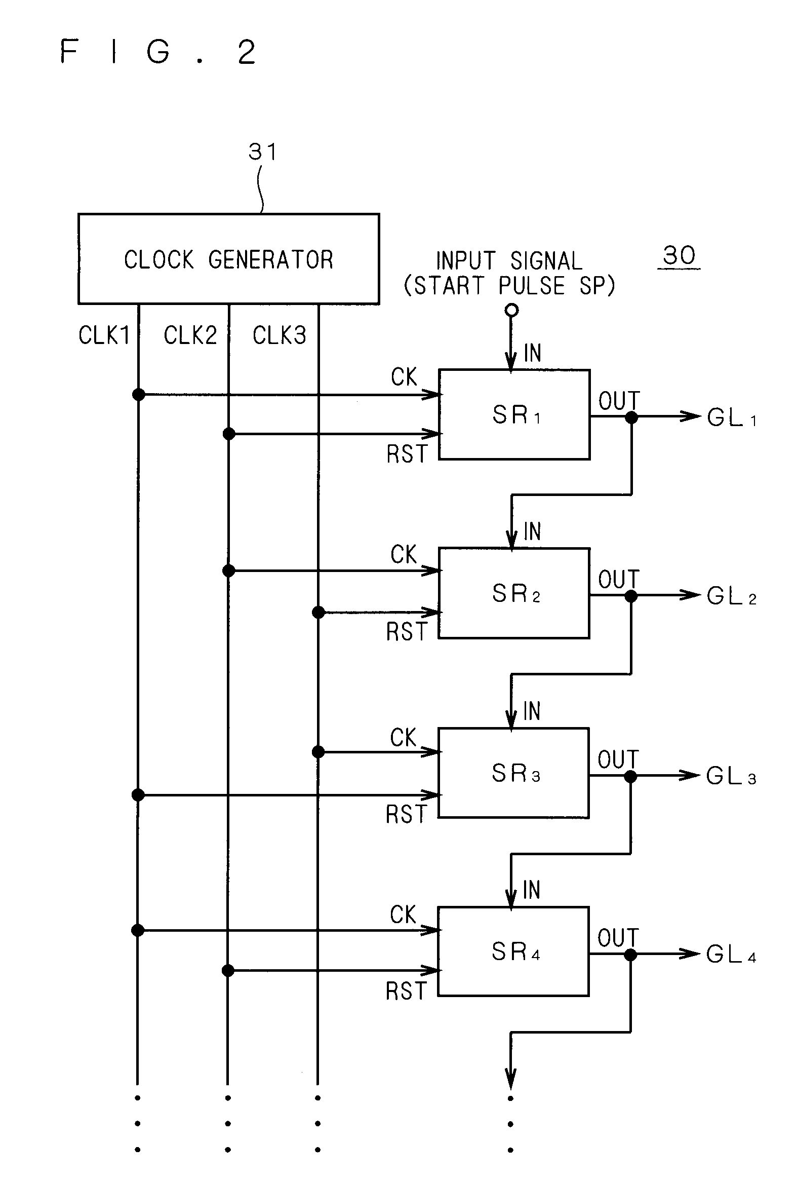
[0058]The liquid crystal display 10 is provided with a liquid crystal array part 20, a gate-line driving circuit (scanning-line driving circuit) 30 and a source driver 40. As will become apparent from the following description, a shift register according to the present invention is mounted on the gate-line driving circuit 30.
[0059]The liquid crystal array part 20 includes a plurality of pixels 25 arrayed in a matrix. The columns of pixels (hereinafter also referred to as “pixel lines”) are respectively provided with gate lines GL1, GL2, . . . (hereinafter also generically referred to as a “gate line GL”), and the rows of pixels (hereinafter also referred to as “pixel rows”) are respectively provided with data lines DL1, DL2, . . . (her...
second preferred embodiment
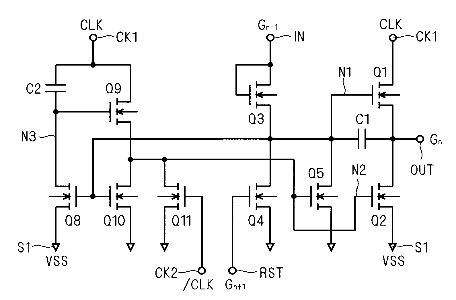
[0142]FIG. 10 is a circuit diagram illustrating the configuration of a unit shift register SR according to a second preferred embodiment of the present invention. In this drawing, elements having similar functions as those shown in FIG. 7 are indicated by the same reference characters. This unit shift register SR is similar to the circuit shown in FIG. 7 except that the transistor Q10 has its gate connected to the output terminal OUT, rather than the node N1.
[0143]The operation of a unit shift register SRn according to the present embodiment is almost similar to that described in the first preferred embodiment. In the first preferred embodiment, the transistor Q10 turns on in the period during which the node N1 is at the H level (from time t1 to time t5 in FIG. 9) to bring the node N2 into the L level, however, in the present embodiment, the transistor Q10 turns on in the period during which the output signal Gn is at the H level (from time t3 to time t4). That is, the transistor Q1...
third preferred embodiment
[0146]FIG. 11 is a circuit diagram illustrating the configuration of a unit shift register according to a third preferred embodiment of the present invention. In this drawing, elements having similar functions as those shown in FIG. 7 are indicated by the same reference characters. The gate node of the transistor Q8, i.e., the input node of the inverter circuit is defined as a “node N1A”. While the gate of the transistor Q1 (node N1) and node N1A are directly connected in the first preferred embodiment (FIG. 7), a transistor Q12 with its gate connected to the node N1A is diode-connected between the nodes N1 and N1A in the unit shift register SR shown in FIG. 11. Further, a transistor Q13 with its gate connected to the input terminal IN is diode-connected between the node N1A and input terminal IN.
[0147]In the unit shift register SRn according to the present embodiment, the node N1 is charged to the H level (VDD−Vth) through the transistor Q3 when the output signal Gn−1 from the imme...
PUM
 Abstract
Description
Claims
Application Information


