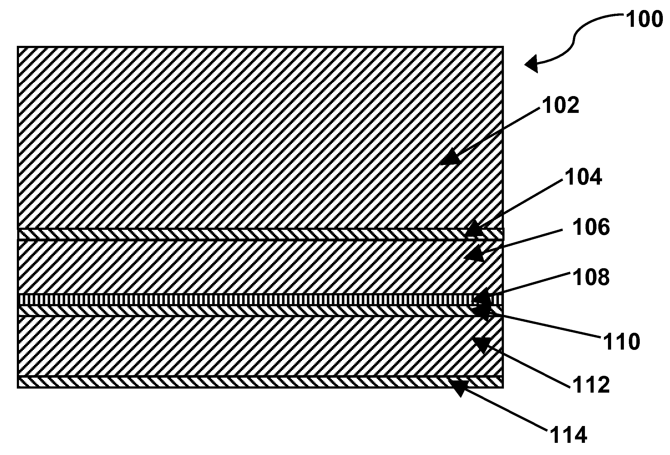
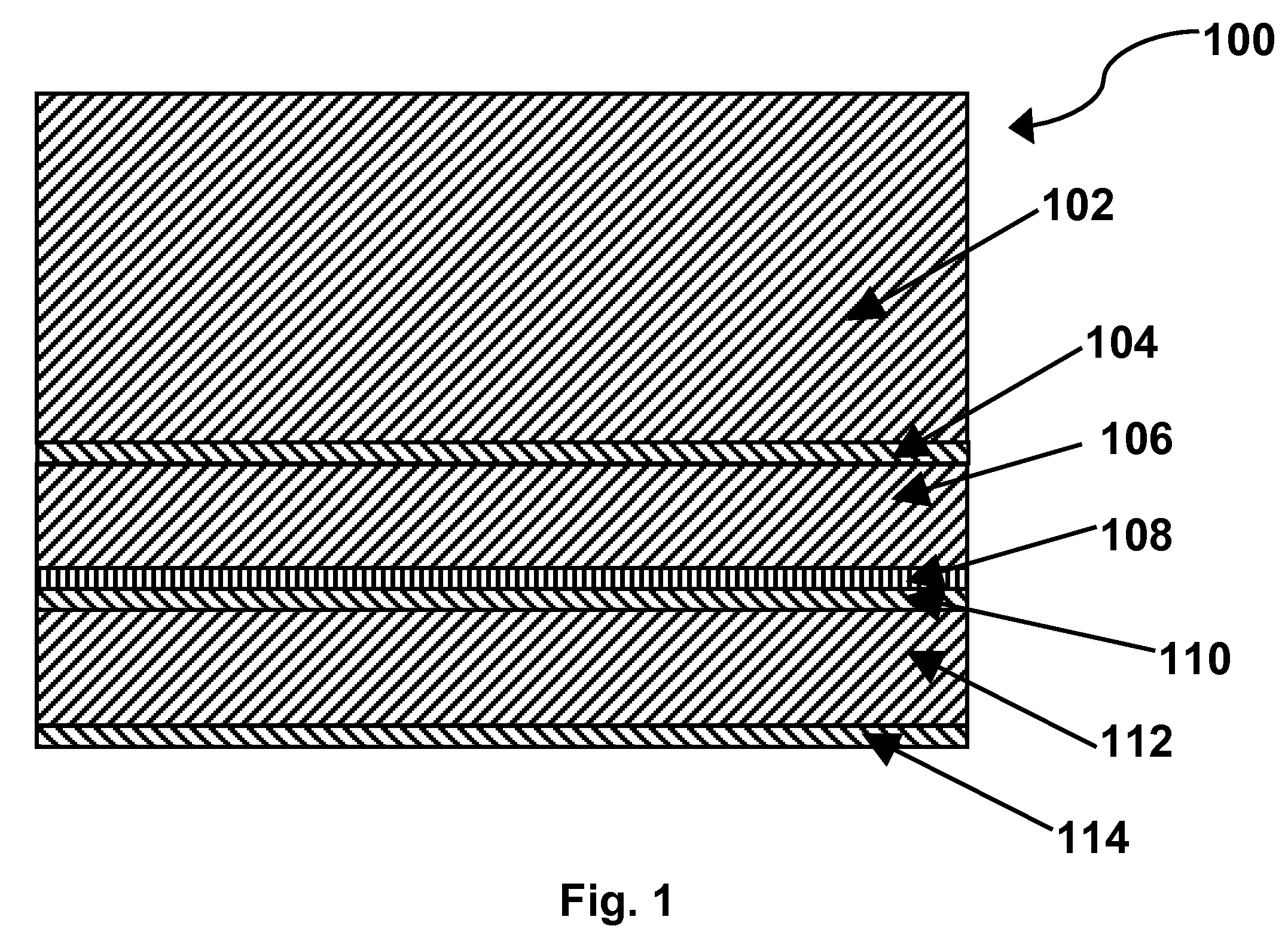
Nevertheless, problems with the long-term
image quality of these displays have prevented their widespread usage.
For example, particles that make up electrophoretic displays tend to settle, resulting in inadequate service-life for these displays.
Such gas-based electrophoretic media appear to be susceptible to the same types of problems due to particle
settling as liquid-based electrophoretic media, when the media are used in an orientation which permits such
settling, for example in a sign where the medium is disposed in a
vertical plane.
Indeed, particle
settling appears to be a more serious problem in gas-based electrophoretic media than in liquid-based ones, since the lower
viscosity of gaseous suspending fluids as compared with liquid ones allows more rapid settling of the electrophoretic particles.
However, the methods used for assembling LCD's cannot be used with
solid electro-optic displays.
This LCD
assembly process cannot readily be transferred to
solid electro-optic displays.
As discussed in the aforementioned U.S. Pat. No. 6,312,304, the manufacture of
solid electro-optic displays also presents problems in that the optical components (the electro -optic medium) and the electronic components (in the
backplane) have differing performance criteria.
Therefore, a process for manufacturing an optical component may not be ideal for manufacturing an
electronic component, and vice versa.
The
processing temperature can be in the range from about 300° C. to about 600° C. Subjecting many optical components to such high temperatures, however, can be harmful to the optical components by degrading the electro-optic medium chemically or by causing mechanical damage.
Electro-optic displays are often costly; for example, the cost of the color LCD found in a
portable computer is typically a substantial fraction of the entire cost of the computer.
However, such equipment is costly and the areas of electro-optic media presently sold may be insufficient to justify dedicated equipment, so that it may typically be necessary to transport the coated medium from a commercial
coating plant to the
plant used for final
assembly of electro-optic displays without damage to the relatively fragile layer of electro-optic medium.
In particular, the electrical
conductivity of the lamination
adhesive layer affects both the low temperature performance and the resolution of the display.
However, increasing the
conductivity of the lamination
adhesive layer in this manner tends to increase pixel blooming (a phenomenon whereby the area of the electro-
optic layer which changes optical state in response to change of
voltage at a pixel
electrode is larger than the pixel
electrode itself), and this blooming tends to reduce the resolution of the display.
Hence, this type of display apparently intrinsically requires a compromise between low temperature performance and
display resolution, and in practice it is usually the low temperature performance which is sacrificed.
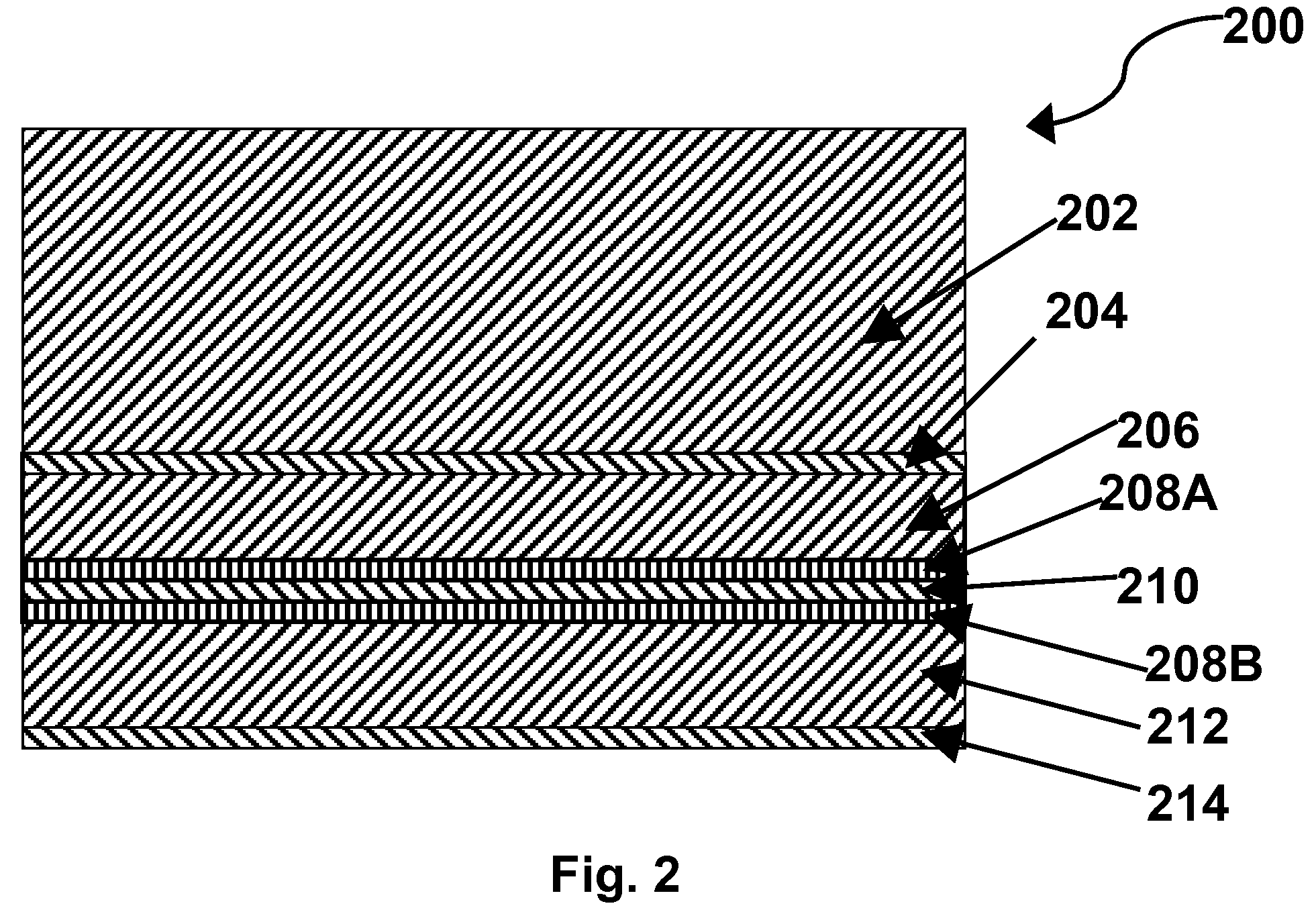
One major challenge in providing such a thin display is sealing the electro-optic medium against the environment, including
radiation.
Providing all these functions in a front sub-assembly thin enough to be used in a highly
flexible display is a matter of considerable difficulty.
While in theory it would be desirable to provide all the necessary functions in a single, monolithic layer, there appears to be no known material capable of providing all these functions in a single layer, and even if such a material could be developed, it would probably be impracticably expensive for use in highly flexible displays.
Using such a multi-layer front sub-assembly, however, exacerbates another problem in the production of highly flexible displays, namely the difficulty of performing
manufacturing operations, including
coating, handling, laminating and assembly operations, on very thin substrates due to the lack of stiffness of such substrates.
These difficulties can be reduced to some extent by using web
processing wherever possible, but final assembly of a highly
flexible display requires lamination of a thin sub-assembly comprising the front sub-assembly, the electro-optic medium and (typically) a lamination
adhesive layer to a thin
backplane, and this lamination normally cannot be performed using web
processing.
Another problem in designing highly flexible displays is the phenomenon of “
creep”.
Unless the
flexible display is carefully designed, the repeated unrolling or unwrapping of such flexible displays is likely to cause the front and rear substrates normally present to move slightly (
creep) relative to one another.
Such
creep is highly undesirable, since it may result in
delamination of various
layers of the display from one another, or introduce differences in electro-optic properties between various portions of the display.
Creep is a particular problem in color displays using color filters, since any movement between a color filter disposed adjacent the viewing surface of the display and the pixel electrodes present near the rear surface of the display destroys the alignment between the color filter elements and the pixel electrodes needed for accurate
color reproduction and thus adversely affects the colors produced by the display.
Such sputtered
ceramic layers are expensive and can constitute a substantial fraction of the overall cost of the display.

