Semiconductor display device

a display device and semiconductor technology, applied in the field of semiconductor display devices, can solve problems such as fluctuation of threshold voltages, and achieve the effects of reducing the number of pins of an fpc, increasing physical impact resistance, and reducing the yield due to connection failure of the fp

Inactive Publication Date: 2010-03-02
SEMICON ENERGY LAB CO LTD
View PDF353 Cites 100 Cited by
  • Summary
  • Abstract
  • Description
  • Claims
  • Application Information

AI Technical Summary

Benefits of technology

[0015]The present invention has been devised in view of the above and other drawbacks, and it is an object of the present invention to provide a semiconductor display device having an interlayer insulating film which can obtain planarity of a surface of the interlayer insulating film while controlling film formation time, can control time for heating treatment for removing moisture in the interlayer insulating film, and can prevent the moisture from being discharged to a film or an electrode adjacent to the interlayer insulating film.

Problems solved by technology

The applicant surmises that plasma damage at the time of the dry etching causes the acrylic film to capture charges, which results in fluctuation of threshold voltages.

Method used


Image

  • Semiconductor display device
  • Semiconductor display device
  • Semiconductor display device

Examples


first embodiment

[0118]In this embodiment, a manufacturing method of a light emitting device which is one of the semiconductor devices of the present invention will be described. Note that, in this embodiment, a method of manufacturing a pixel portion and a storage capacitor included in a circuit provided around the pixel portion will be described in detail.

[0119]First, as shown in FIG. 8A, a base film 5002 including an insulating film such as a silicon oxide film, a silicon nitride film, or a silicon oxide nitride film is formed on a substrate 5001 including glass such as barium borosilicate glass or aluminoborosilicate glass represented by #7059 glass, #1737 glass, and the like of Coming Corporation. For example, a silicon oxide nitride film 5002a produced from SiH4, NH3, and N2O is formed with a thickness of 10 to 200 nm (preferably 50 to 100 nm) by the plasma CVD method, and a silicon oxide nitride hydrogenate film 5002b produced from SiH4 and N2O is likewise formed with a thickness of 50 to 200...

second embodiment

[0176]In this embodiment, a structure of a light emitting device having a sectional structure different from that of the light emitting device shown in the first embodiment will be described.

[0177]In a light emitting device shown in FIG. 13A, after forming a second inorganic insulating film 7500, a transparent conductive film is formed and patterned before forming a contact hole, whereby a pixel electrode 7501 is formed. Then, a gate insulating film 7502, a first inorganic insulating film 7503, and the second inorganic insulating film 7500 are etched in an opening part of an organic resin film 7504 to form the contact hole, and a wiring 7506 electrically connecting a TFT 7505 and the pixel electrode 7501 is formed.

[0178]In this way, by forming the pixel electrode 7501 before forming the wiring 7506, a process of polishing a surface of the pixel electrode before forming the wiring 7506 can be provided.

[0179]In a light emitting device shown in FIG. 13B, after forming a second inorgani...

third embodiment

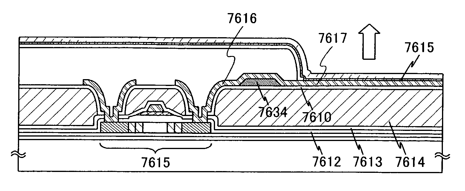
[0192]In this embodiment, electric connection between an capacitor electrode for lowering a resistance of a cathode and a terminal for FPC to be connected to a terminal of an FPC will be described.

[0193]FIG. 15A shows a sectional view of a light emitting device at a point when, after a third interlayer insulating film 6201 is formed on a second interlayer insulating film 6200 having an opening part, an capacitor electrode 6202 is formed on the third interlayer insulating film 6201. The capacitor electrode 6202 is formed of a material having a wiring resistance lower than that of a cathode to be formed later.

[0194]Note that an electrode for FPC 6204 formed of the same conductive film as a gate electrode 6203 of a TFT is formed in an opening part of the second interlayer insulating film 6200. In addition, a terminal for FPC 6205 formed of the same transparent conductive film as a pixel electrode 6206 is formed on the electrode for FPC 6204.

[0195]At the point of FIG. 15A, the terminal ...


PUM

PropertyMeasurementUnit
angleaaaaaaaaaa
angleaaaaaaaaaa
curvature radiusaaaaaaaaaa

Abstract

It is an object of the present invention to provide a semiconductor display device having an interlayer insulating film which can obtain planarity of a surface while controlling film formation time, can control treatment time of heating treatment with an object of removing moisture, and can prevent moisture in the interlayer insulating film from being discharged to a film or an electrode adjacent to the interlayer insulating film. An inorganic insulating film containing nitrogen, which is less likely to transmit moisture compared with an organic resin, is formed so as to cover a TFT. Next, an organic resin film containing photosensitive acrylic resin is applied to the organic insulting film, and the organic resin film is partially exposed to light to be opened. Thereafter, an inorganic insulting film containing nitrogen, which is less likely to transmit moisture compared with an organic resin, is formed so as to cover the opened organic resin film. Then, in the opening part of the organic resin film, a gate insulating film and the two layer inorganic insulating film containing nitrogen are opened partially by etching to expose an active layer of the TFT.

Description

BACKGROUND OF THE INVENTION[0001]1. Field of the Invention[0002]The present invention relates to a semiconductor display device in which an organic resin film is used as an interlayer insulating film.[0003]2. Description of the Related Art[0004]In recent years, a technology for forming a TFT on a substrate has achieved a great advance, and application of the technology to an active matrix semiconductor display device which is one of semiconductor devices has been in progress. In particular, a TFT using a polycrystalline semiconductor film can operate at a high speed because it has field effect mobility higher than that of a conventional TFT using an amorphous semiconductor film. Thus, it is possible to perform control of pixels, which has been conventionally performed by a drive circuit provided outside a substrate, with a drive circuit formed on a substrate identical with a substrate on which the pixels are formed.[0005]A TFT includes an active layer, which is obtained by adding im...

Claims


Application Information

Patent Timeline
Patent Type & Authority Patents(United States)
IPC IPC(8): H01L29/04G02F1/1333G02F1/1362G02F1/1368G09F9/30H01L21/77H01L21/84H01L27/12H01L27/13H01L27/32H01L29/786H01L51/50H01L51/52
CPCG02F1/136227H01L27/12H01L27/124H01L27/1248H01L27/1244H01L33/52H01L27/1214H01L27/1255H01L27/3246H01L27/3276H01L27/13H01L51/5237G02F1/133357H10K59/122H10K59/123H10K59/124H10K59/131H10K50/84H10K50/844
Inventor YAMAZAKI, SHUNPEIMURAKAMI, SATOSHIHAYAKAWA, MASAHIKOKATO, KIYOSHIOSAME, MITSUAKI
Owner SEMICON ENERGY LAB CO LTD
Why Eureka
Try Eureka