Laser diode

a laser diode and diode technology, applied in the field of laser diodes, can solve the problems of high material cost, difficult assembly, and large increase in material cost of gan substrates, so as to reduce the size of the first light emitting device, reduce the size of gan substrates which need a relatively expensive material cost, and reduce the material cost

Inactive Publication Date: 2010-03-02
SONY CORP
View PDF28 Cites 5 Cited by
  • Summary
  • Abstract
  • Description
  • Claims
  • Application Information

AI Technical Summary

Benefits of technology

[0009]In view of foregoing, in the invention, it is desirable to provide a laser diode which can be easily assembled at a low material cost.
[0012]According to the laser diode of the embodiment of the invention, the first substrate side of the first light emitting device and the laser structure side of the second light emitting device are electrically connected to the support base, and thereby electrical power from the support base side can be supplied. Therefore, it is not necessary to provide a region for connecting a wire led out from the electrical power source on the first light emitting device. Thereby, the size of the first light emitting device can be decreased by the above region which has been saved. Here, for example, when the first substrate is made of a GaN substrate and the second substrate is made of a GaAs substrate, a size of the GaN substrate which needs a relatively expensive material cost can be decreased. In the result, the material cost can be reduced.
[0013]Further, by layering the first light emitting device and the second light emitting device in this order on the support base in a manner that the respective laser structures are opposed to each other, the distance between the light emitting points of the first light emitting device and the second light emitting device is reduced. Therefore, design margin of optical pickup becomes favorable, and the laser diode can be easily assembled.

Problems solved by technology

However, a material cost for the GaN substrate is greatly higher than that for the GaAs substrate.
Therefore, when the size of the first light emitting device is increased, the material cost becomes greatly high.
As above, in the structure of Japanese Unexamined Patent Application Publication No. 2003-298193, there are disadvantages that assembly is not easy and the material cost is greatly high.

Method used


Image

  • Laser diode
  • Laser diode
  • Laser diode

Examples


first embodiment

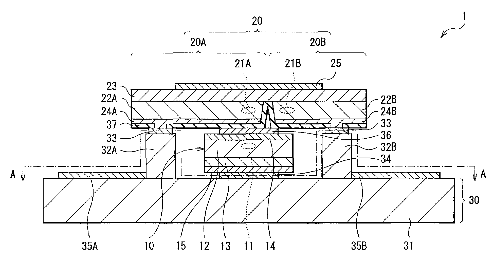
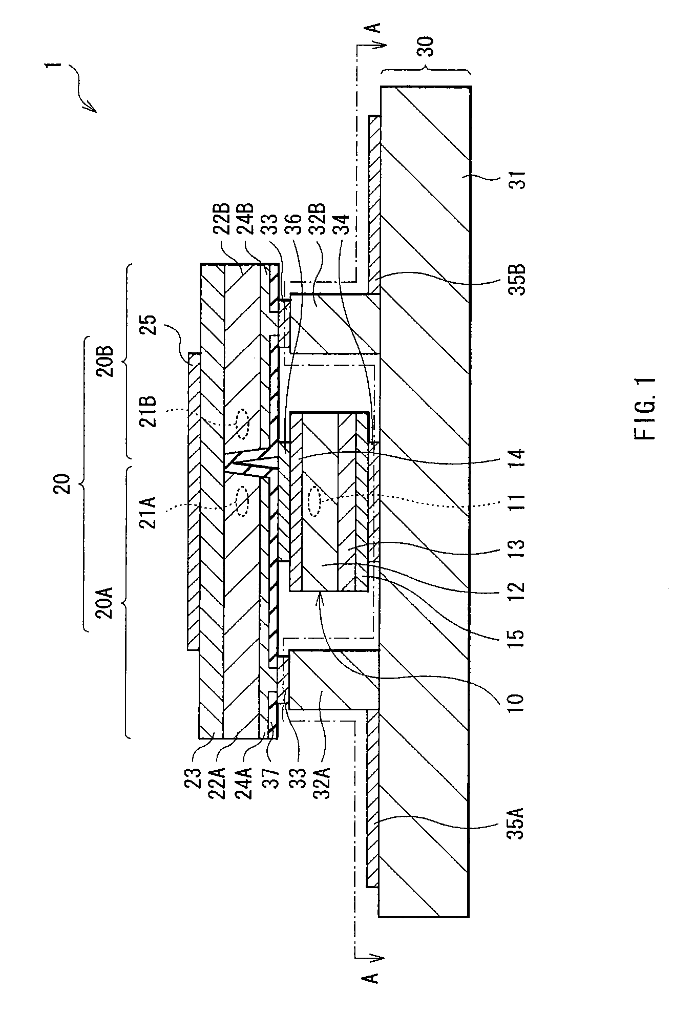
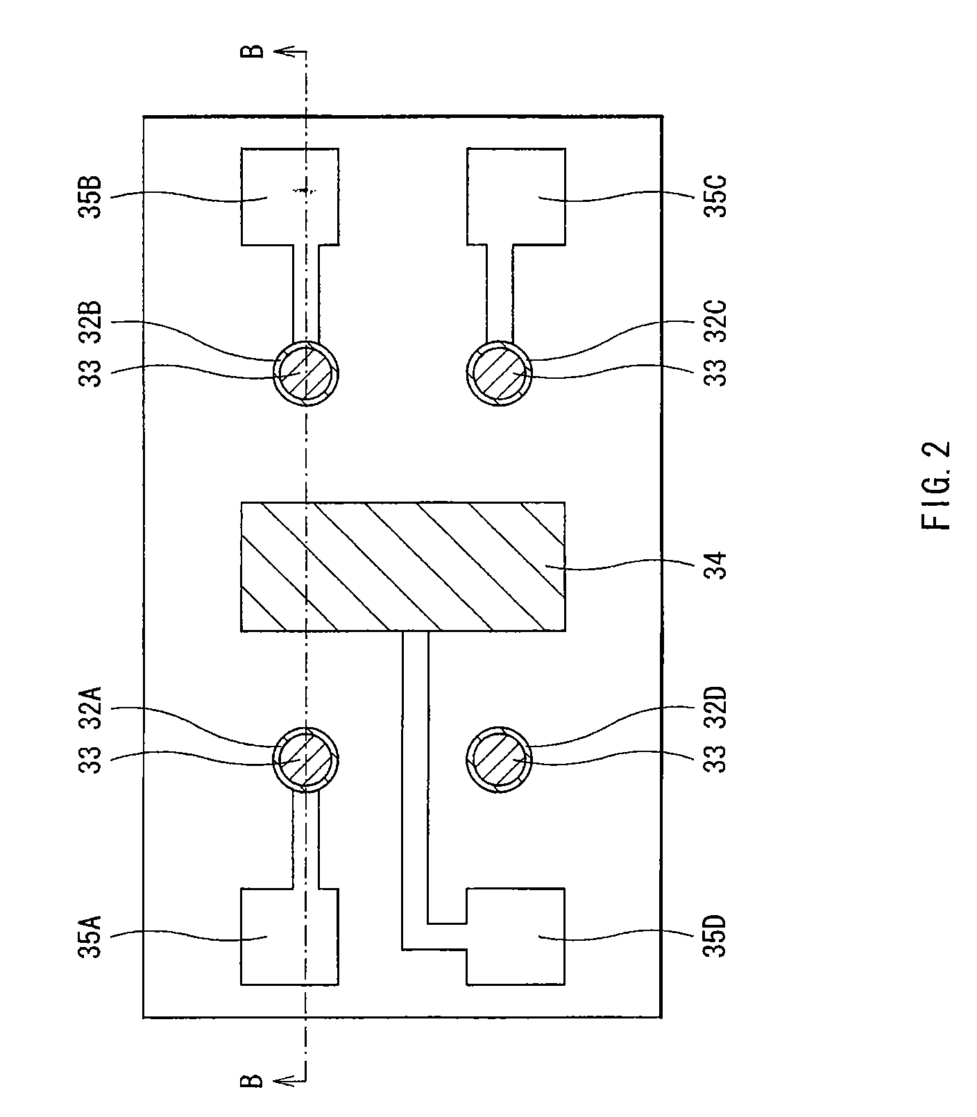
[0028]FIG. 1 shows a cross sectional structure of a laser diode 1 according to a first embodiment of the invention. FIG. 2 shows a cross sectional structure taken along arrows A-A of the laser diode 1 of FIG. 1. The cross sectional structure of FIG. 1 corresponds to a cross sectional structure taken along arrows B-B of FIG. 2. FIG. 3 and FIG. 4 respectively show a top face structure and a side face structure of a laser diode 9 of this embodiment. The laser diode 9 is structured by mounting the laser diode 1 of FIG. 1 to a heat block 60 and connection terminals 70. FIG. 1 to FIG. 4 show models of the laser diode 1 and the laser diode 9, and the dimensions and the shapes in the figures are different from those used actually.

[0029]The laser diode 1 is a device in which a chip-shaped first light emitting device 10 and a chip-shaped second light emitting device 20 are layered in this order on a support base 30. The first light emitting device 10 includes a laser structure 12 forming a li...

second embodiment

[0073]FIG. 5 shows a cross sectional structure of a laser diode 2 according to a second embodiment of the invention. In FIG. 5, internal structures of the first light emitting device 10 and the second light emitting device 20 are omitted.

[0074]The laser diode 2 is different from the foregoing first embodiment in that the laser diode 2 includes a bump 42 (deformable conductive part) instead of the columnar post 32 and the adhesive layer 33. Therefore, a description will be hereinafter mainly given of differences from the first embodiment, and structures, actions, and effects similar to those of the first embodiment will be omitted as appropriate.

[0075]The bump 42 contains a deformable conductive material such as gold (Au). The bump 42 supports the second light emitting device 20, and supplies electrical power from the support base 30 side to the second light emitting device 20 similarly to the columnar post 32 of the first embodiment. Gold (Au) is a material with superior heat conduc...

third embodiment

[0079]FIG. 9 shows a cross sectional structure of a laser diode 3 according to a third embodiment of the invention. FIG. 10 shows a step of arranging the first light emitting device 10 and the second light emitting device 20 on a support base 40. In FIG. 9 and FIG. 10, internal structures of the first light emitting device 10 and the second light emitting device 20 are omitted.

[0080]The laser diode 3 is different from the foregoing first embodiment in that the laser diode 3 includes a heat conductive part 41 provided with a groove 41A instead of the columnar post 32. Therefore, a description will be hereafter mainly given of differences from the first embodiment, and structures, actions, and effects similar to those of the first embodiment will be omitted as appropriate.

[0081]The heat conductive part 41 has a groove 41A provided in a region opposed to the first light emitting device 10 and a side groove 41B provided in the both sides of the groove 41A. The groove 41A is composed of ...


PUM


Abstract

A laser diode which can be easily assembled at low material cost is provided. A first light emitting device having a laser structure on a substrate, a second light emitting device having laser structures on a substrate, and a support base are provided. The first light emitting device and the second light emitting device are layered in this order on the support base in a manner that the respective laser structures of the first light emitting device and the second light emitting device are opposed to each other. A substrate side of the first light emitting device and a laser structure side of the second light emitting device are electrically connected to the support base.

Description

CROSS REFERENCES TO RELATED APPLICATIONS[0001]The present invention contains subject matter related to Japanese Patent Application JP 2005-229321 filed in the Japanese Patent Office on Aug. 8, 2005, the entire contents of which being incorporated herein by reference.BACKGROUND OF THE INVENTION[0002]1. Field of the Invention[0003]The present invention relates to a laser diode including a plurality of light emitting devices such as a two-wavelength laser and a three-wavelength laser.[0004]2. Description of the Related Art[0005]In recent years, in the field of a laser diode (LD), a multi-wavelength laser having a plurality of light emitting portions with different light emitting wavelengths on the same substrate (or base) has been actively developed. The multi-wavelength laser is used as, for example, a light source for optical disk devices.[0006]In such optical disk devices, laser light in the 700 nm band is used for reproduction in a CD (Compact Disk), and is used for recording and r...

Claims


Application Information

Patent Timeline
Patent Type & Authority Patents(United States)
IPC IPC(8): H01S5/00H01S5/02315
CPCH01S5/4025H01S5/02236H01S5/0224H01S5/405H01S5/4087H01L2224/48247H01L2224/4917H01S5/0234H01S5/0233H01S5/0235H01S5/02315
Inventor SATO, KEIJIHAYASHI, RYUICHIROOIKAWA, KENJIASANO, TAKEHARU
Owner SONY CORP
Why Eureka
Try Eureka