Method for manufacturing photoelectric conversion device

a technology of photoelectric conversion and manufacturing method, which is applied in the manufacture of final products, basic electric elements, climate sustainability, etc., can solve the problems of reducing the revenues of the production plant for solar cells, the sourcing cost of silicon wafers is increased, and the supply cannot meet the demand. , to achieve the effect of improving conversion efficiency and reducing the surface reflectivity of single crystal semiconductor layers

Inactive Publication Date: 2010-03-09
SEMICON ENERGY LAB CO LTD
View PDF29 Cites 26 Cited by
  • Summary
  • Abstract
  • Description
  • Claims
  • Application Information

AI Technical Summary

Benefits of technology

[0009]In view of such circumstances, it is an object of the present invention to provide a method for manufacturing a photoelectric conversion device typified by a solar cell, having an excellent photoelectric conversion characteristic with a silicon semiconductor material effectively utilized.
[0013]In accordance with the present invention, the single crystal semiconductor layer bonded to the supporting substrate is irradiated with the laser beam in the atmosphere containing oxygen so that the surface of the single crystal semiconductor layer can be made rough. As a result, the surface reflectivity of the single crystal semiconductor layer can be decreased. Using this single crystal semiconductor layer as a photoelectric conversion layer, light trapping effect is produced and the conversion efficiency can be improved.

Problems solved by technology

That is, the following problem becomes obvious: even though the production capability is high enough, the supply cannot nevertheless keep up with the demand because of the shortage of material.
Or, the sourcing cost of a silicon wafer is increased, which decreases revenues in the production plant for solar cells.

Method used


Image

  • Method for manufacturing photoelectric conversion device
  • Method for manufacturing photoelectric conversion device
  • Method for manufacturing photoelectric conversion device

Examples


embodiment mode 1

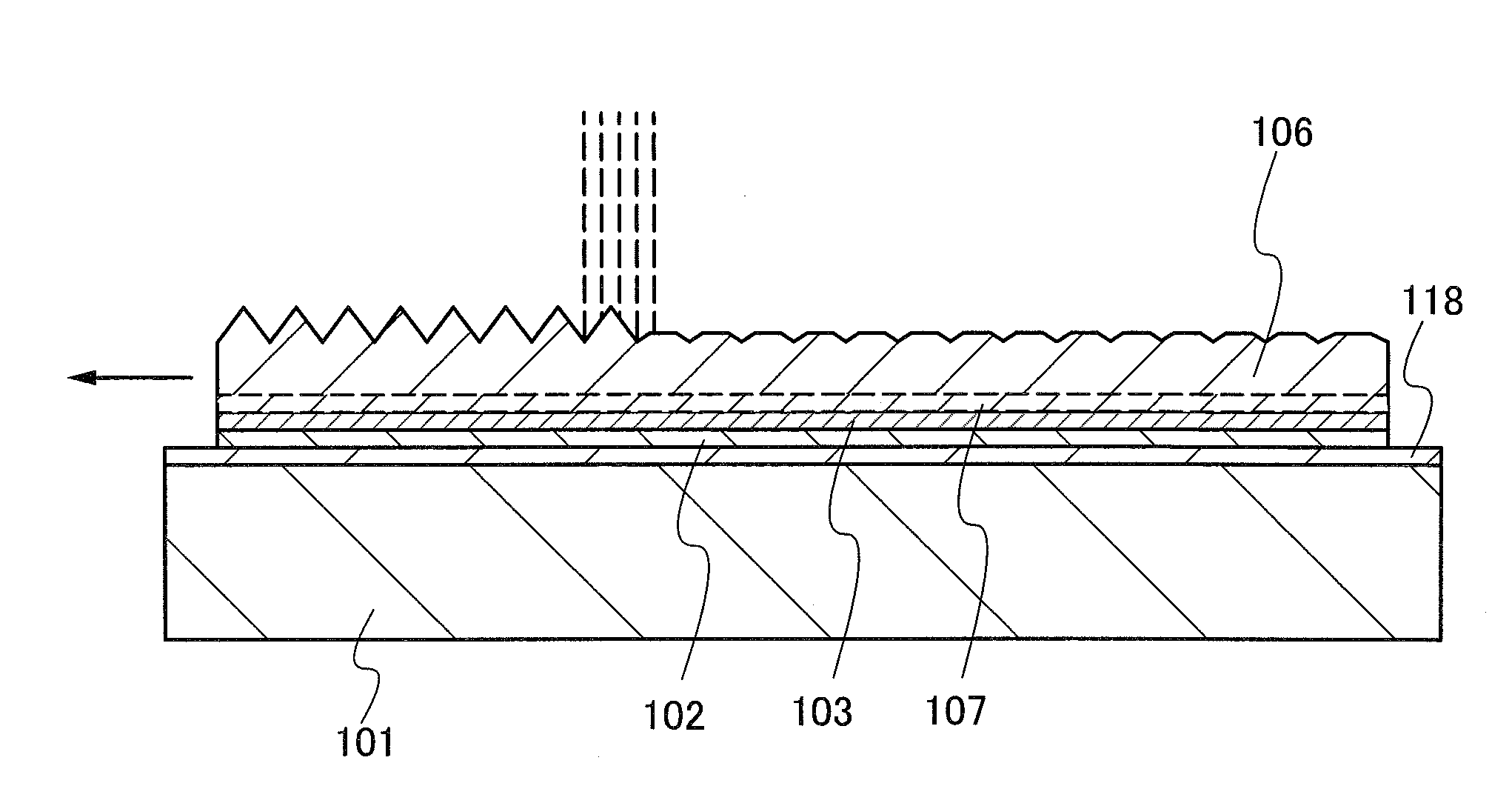
[0036]Described using drawings will be a method for manufacturing a photoelectric conversion device, in which a single crystal semiconductor thin layer is separated from a single crystal semiconductor substrate and transferred to a substrate having an insulating surface or an insulating supporting substrate.

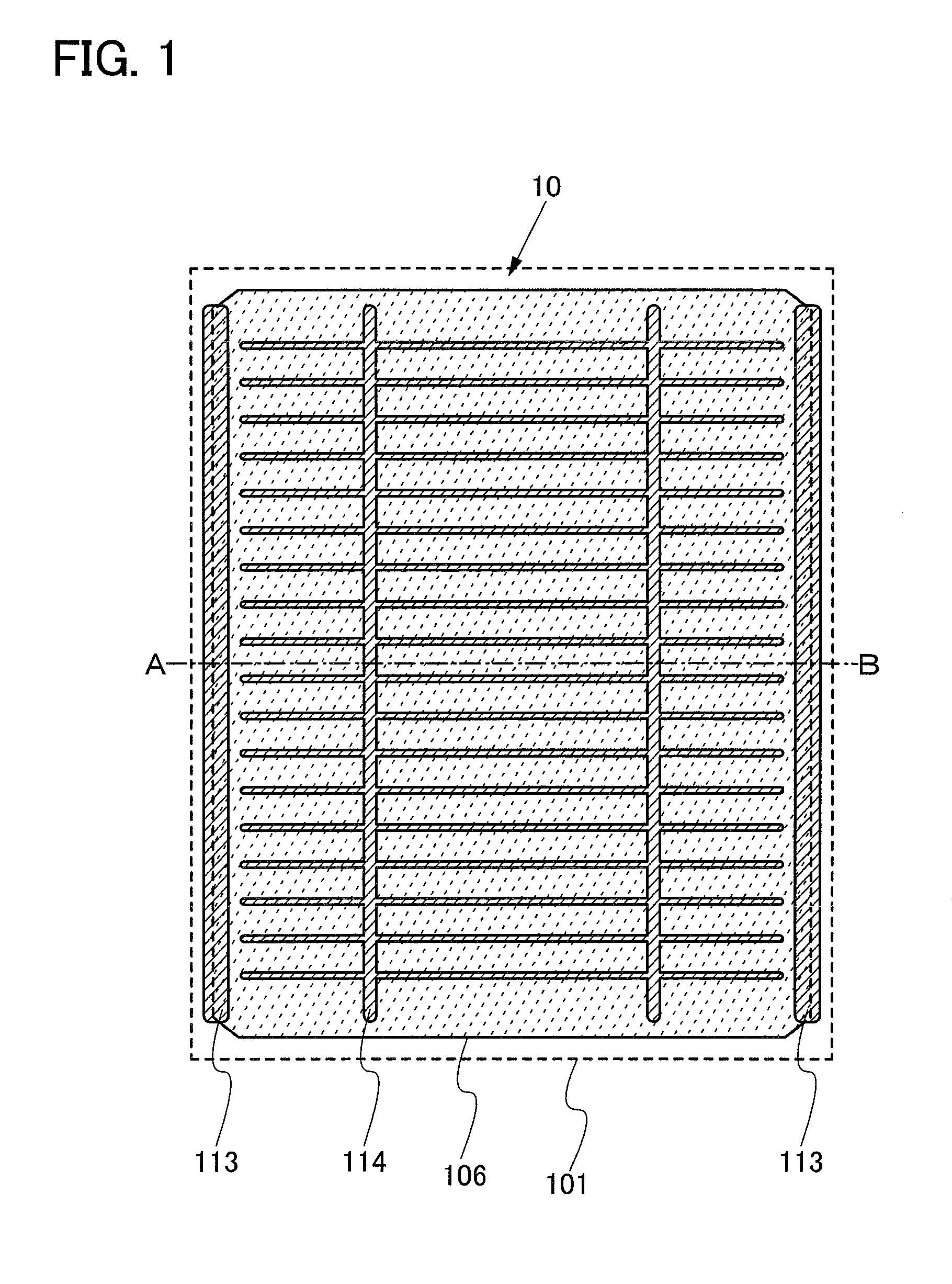
[0037]FIG. 1 is a plan view of a photoelectric conversion device 10 of this embodiment mode. This photoelectric conversion device 10 produces a photoelectric effect by light incidence into a single crystal semiconductor layer 106 fixed on a supporting substrate 101. The single crystal semiconductor layer 106 is provided with an impurity semiconductor layer for forming an internal electrical-field. As the single crystal semiconductor layer 106, single crystal silicon is typically used. Alternatively, a polycrystalline semiconductor layer can be used instead of the single crystal semiconductor layer 106; in this case, polycrystalline silicon is used.

[0038]In FIG. 1, the surface sid...

embodiment mode 2

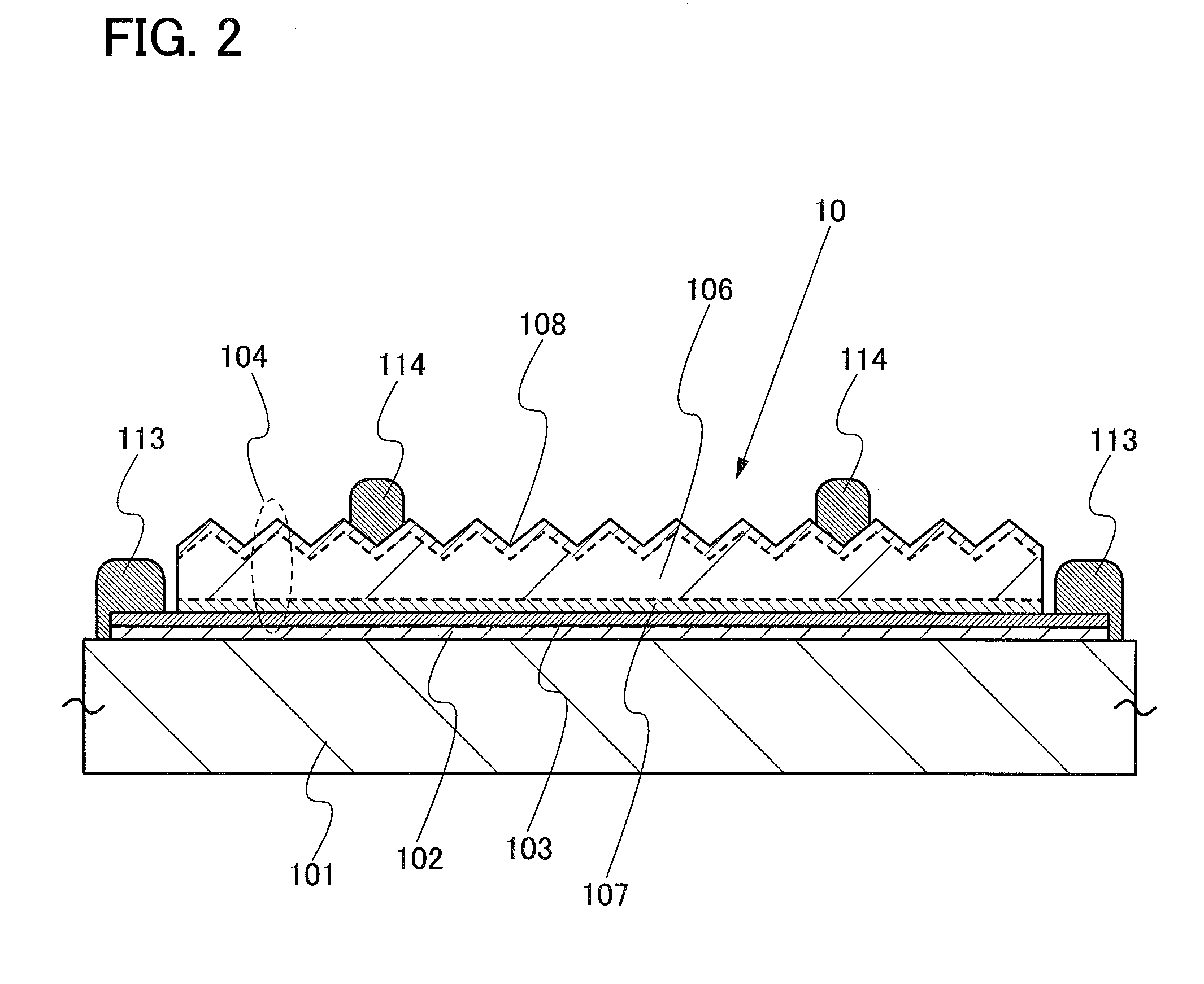
[0054]Next, a method for manufacturing the photoelectric conversion device 10 with its cross-sectional structure along section line A-B of FIG. 1 corresponding to the structure shown in FIG. 2 described in Embodiment Mode 1 will be described.

[0055]A semiconductor substrate 115 shown in FIG. 5A is a substrate with a shape approximately a quadrangular shape, cut out from a circular single crystal semiconductor substrate. The semiconductor substrate 115 is typically single crystal silicon and preferably has its surface polished to have a mirror surface. It is preferable that a protection film 116 be formed of silicon oxide or silicon nitride and a chemical vapor deposition method is used for the formation.

[0056]The first impurity semiconductor layer 107 having one conductivity type is formed in the semiconductor substrate 115. For example, boron is added as an impurity element which imparts one conductivity type so that the first impurity semiconductor layer 107 is formed to have p-typ...

embodiment mode 3

[0091]In this embodiment mode, manufacturing steps which are different from those in Embodiment Mode 2 will be described with reference to FIGS. 11A to 11C. The protection film 116 is formed and the first impurity semiconductor layer 107 is formed in the semiconductor substrate 115 (FIG. 11A), and then the damaged layer 117 is formed with the protection film 116 left (FIG. 11B). After that, the protection film 116 is removed and the first electrode 103 is formed (FIG. 11C). The process of this embodiment mode make it possible to effectively use the protection film 116. That is, the protection film 116 is removed after the formation of the damaged layer 117, so that a bonding surface of the semiconductor substrate 115 can be flat. It is preferable that the protection film 116 be provided to have a thickness of 50 to 200 nm. In addition, the damaged layer 117 is formed by introducing cluster ions of hydrogen through the first impurity semiconductor layer 107, so that hydrogenation of ...


PUM


Abstract

A method for manufacturing a photoelectric conversion device typified by a solar cell, having an excellent photoelectric conversion characteristic with a silicon semiconductor material effectively utilized. The point is that the surface of a single crystal semiconductor layer bonded to a supporting substrate is irradiated with a pulsed laser beam to become rough. The single crystal semiconductor layer is irradiated with the pulsed laser beam in an atmosphere containing an inert gas and oxygen so that the surface thereof is made rough. With the roughness of surface of the single crystal semiconductor layer, light reflection is suppressed so that incident light can be trapped. Accordingly, even when the thickness of the single crystal semiconductor layer is equal to or greater than 0.1 μm and equal to or less than 10 μm, path length of incident light is substantially increased so that the amount of light absorption can be increased.

Description

BACKGROUND OF THE INVENTION[0001]1. Field of the Invention[0002]The present invention relates to a method for manufacturing a photoelectric conversion device using a single crystal semiconductor or a polycrystalline semiconductor.[0003]2. Description of the Related Art[0004]Total production of solar cells in the world in 2005 was 1,759 MW, which is an increase of 147% as compared to that in the previous fiscal year. Single-crystal-silicon solar cells and polycrystalline silicon solar cells account for a large part of the production of solar cells.[0005]Silicon semiconductors are resources that are widely used not only in the solar cell industry but also in the semiconductor industry for memories, microprocessors, and the like. Therefore, with the year-by-year increase of production of solar cells, the shortage of supply of polycrystalline silicon, which is the material of silicon, and the resulting rise in the price of a silicon wafer have become problems in the industry.[0006]The t...

Claims


Application Information

Patent Timeline
Patent Type & Authority Patents(United States)
IPC IPC(8): H01L21/00
CPCH01L31/02168H01L31/0236H01L31/0725H01L31/1864H01L31/022425H01L31/028H01L31/036H01L31/03682H01L31/1804Y02E10/50H01L31/02363Y02P70/50
Inventor ARAI, YASUYUKI
Owner SEMICON ENERGY LAB CO LTD
Why Eureka
Try Eureka