Multi-step process for forming a metal barrier in a sputter reactor

a metal barrier and sputter reactor technology, applied in the direction of vacuum evaporation coating, electrolysis components, coatings, etc., can solve the problem that the bias optimization alone has the difficulty of relatively narrow process window, and the sputter tantalum flux has a large horizontal velocity component towards the wafer center, so as to reduce the stray magnetic field, and enhance the effect of magnetic shielding

Active Publication Date: 2010-03-30
APPLIED MATERIALS INC
View PDF20 Cites 15 Cited by
  • Summary
  • Abstract
  • Description
  • Claims
  • Application Information

AI Technical Summary

Benefits of technology

[0021]The invention is also useful for reducing stray magnetic fields extending far outside the sputter reactor, possibly affecting other reactors. The magnetic shielding is enhanced by a magnetic core between the coils and a specified ratio of counter rotating coil currents between the inner and outer coils.
[0022]The quadruple electromagnetic coil array may be wound on a winding spool. The two inner coils are first wound with a non-magnetic radial separator between them. An tubular, axially extending separator is slid over the outside of the inner coils and it includes another non-magnetic radial separator. The outer two coils are wound over the tubular separator. In some embodiments, the tubular separator is advantageously formed of magnetic material, thereby reducing stray magnetic field outside the chamber and reducing the currents needed for a given magnetic field strength inside the chamber.
[0023]The multiple-coil array may be cooled by water or other refrigerant circulating through a helical cooling coil fixed to thermally contact at least two of the electromagnetic coils, for example, on the radial exterior. A metallic coil separator facilitates thermal transfer from the radially outer cooling coil to the inner coils.
[0024]The invention also includes a multi-step process practiced in such a sputter reactor depositing a barrier layer including an etching step. An embodiment of the multi-step process includes the sputter deposition of a barrier layer formed of refractory metal, such as tantalum, and its nitride under high target powering to promote sputter ionization and strong wafer biasing to increase the ion energy and directionality, thereby providing high sidewall coverage and low bottom coverage in the via. The nitride is preferably sputtered with higher energy than the refractory metal so that the nitride bottom coverage is low, possibly zero, and can further clean the underlying contact. An argon etch step is performed with minimal target power and significant RF power to the coil. A flash sputter deposition of the refractory metal is performed to produce high neutral sputter flux to assure field coverage.

Problems solved by technology

However, this approach causes the sputtered tantalum flux to have a large horizontal velocity component towards the wafer center.
Bias optimization by itself has the difficulty that the process window is relatively narrow.
However, optimization is still difficult because the magnetization amount is not easily changed.
Furthermore, solenoid coils introduce an issue of stray magnetic fields being produced outside the chamber.
As the feature sizes on integrated circuits continue to decrease and the depth and thicknesses of various layers also decrease, the use of highly energetic sputter ions in achieving sidewall coverage and removing bottom barrier layers in high aspect-ration vias is disfavored because of the damage they may cause.
Nonetheless, the selective deposition and removal are still needed.
Wafer transfer and chamber pump down present high overhead.
Heretofore, chambers have not been optimized for multiple operating modes.

Method used


Image

  • Multi-step process for forming a metal barrier in a sputter reactor
  • Multi-step process for forming a metal barrier in a sputter reactor
  • Multi-step process for forming a metal barrier in a sputter reactor

Examples


Embodiment Construction

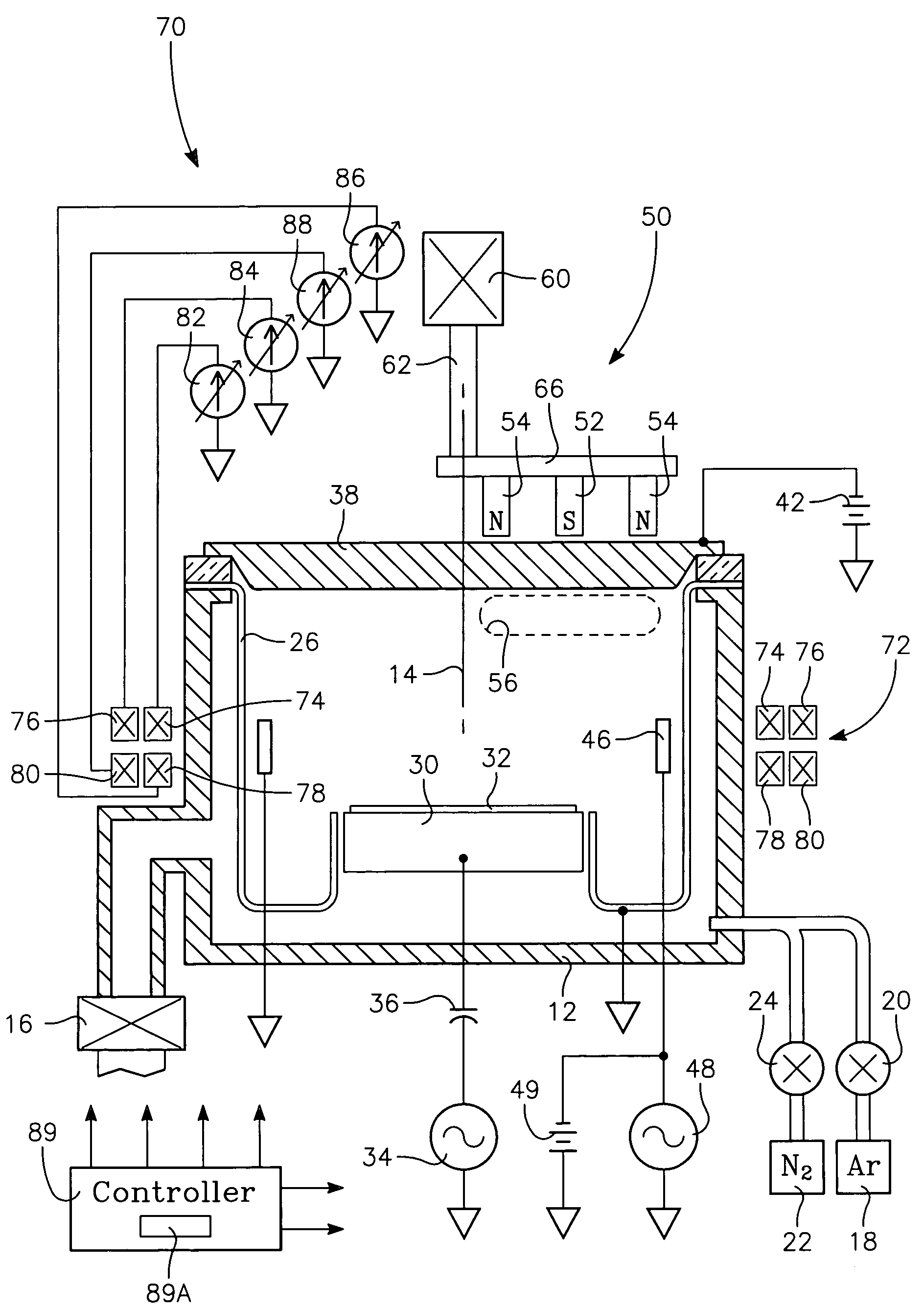
[0040]One aspect of the invention relies upon multiple solenoid coils or electromagnets, preferably arranged in an array, to flexibly tailor the magnetic field within the sputter chamber in multiple steps of a sputter and etch process enabled by the invention. A plasma reactor 70 illustrated schematically in cross section in FIG. 8 includes a quadruple electromagnet array 72 positioned generally in back of the RF coil 46. The quadruple electromagnet array 72 includes four solenoidal coils 74, 76, 78, 80 wrapped generally circularly symmetrically about the central axis 14 of the reactor 70. The coils 74, 76, 78, 80 are preferably arranged in a two-dimensional array extending around the central axis. The nomenclature is adopted of the top inner magnet (TIM) 74, top outer magnet (TOM) 76, bottom inner magnet (BIM) 78, and bottom outer magnet (BOM) 80. The coils 74, 76, 78, 80 may each be separately powered, for example, by respective variable DC current supplies 82, 84, 86, 88, prefera...


PUM

PropertyMeasurementUnit
pressureaaaaaaaaaa
magnetic fieldsaaaaaaaaaa
distanceaaaaaaaaaa

Abstract

A multi-step process performed in a plasma sputter chamber including sputter deposition from the target and argon sputter etching of the substrate. The chamber includes a quadruple electromagnetic coil array coaxially arranged in a rectangular array about a chamber axis outside the sidewalls of a plasma sputter reactor in back of an RF coil within the chamber. The coil currents can be separately controlled to produce different magnetic field distributions, for example, between a sputter deposition mode in which the sputter target is powered to sputter target material onto a wafer and a sputter etch mode in which the RF coil supports the argon sputtering plasma. A TaN / Ta barrier is first sputter deposited with high target power and wafer bias. Argon etching is performed with even higher wafer bias. A flash step is applied with reduced target power and wafer bias.

Description

RELATED APPLICATION[0001]This application is a continuation in part of Ser. No. 10 / 950,349, filed Sep. 23, 2004, which claims benefit of U.S. provisional application 60 / 574,905, filed May 26, 2004.FIELD OF THE INVENTION[0002]The invention relates generally to plasma processing of substrates. In particular, the relates to the RF coils and auxiliary magnets, for example, electromagnets used in a sputter reactor, most particularly in a multi-step process.BACKGROUND ART[0003]Sputtering, alternatively called physical vapor deposition (PVD), is used to deposit several different layers of metals and related materials in the fabrication of semiconductor integrated circuits. In one demanding application, a thin barrier layer is sputtered onto the walls and bottom of a narrow hole etched into and often through an inter-level dielectric layer, most typically composed of silicon oxide or similar oxide materials. The remainder of the hole is then filled with a metal to serve an electrical connec...

Claims


Application Information

Patent Timeline
Patent Type & Authority Patents(United States)
IPC IPC(8): C23C14/00C23C14/04C23C14/06C23C14/16C23C14/32C23C14/35C23C16/00C23F1/02C23F4/00H01J37/32H01J37/34H01L21/285H01L21/768
CPCC23C14/046C23C14/0641C23C14/165C23C14/358C23F4/00H01J37/321H01L21/76865H01J37/3266H01J37/32688H01J37/3408H01L21/2855H01L21/76844H01L21/76846H01J37/32623C23C14/34C23C14/35
Inventor GUNG, TZA-JINGFU, XINYUSUNDARRAJAN, ARVINDHAMMOND, IV, EDWARD P.GOPALRAJA, PRABURAMFORSTER, JOHN C.PERRIN, MARK A.GILLARD, ANDREW S.
Owner APPLIED MATERIALS INC
Why Eureka
Try Eureka