
Semiconductor device fabrication method

a technology of semiconductor devices and fabrication methods, applied in the field of hf (hydrogen fluoride) cleaning technology, can solve problems such as deteriorating product quality

Inactive Publication Date: 2010-03-30
LAPIS SEMICON CO LTD
View PDF3 Cites 2 Cited by
  • Summary
  • Abstract
  • Description
  • Claims
  • Application Information

AI Technical Summary

Benefits of technology

The present invention provides a method for preventing corrosion of circuit elements during cleaning steps in semiconductor device fabrication. The method involves dipping the semiconductor substrate, with circuit elements and protective film, into pure water to allow water to filter into the gap between the resist and substrate. The water is then evaporated at high temperature to generate a strong surface tension that prevents the hydrogen fluoride aqueous solution from filtering into the gap. A surface active agent may be used to remove airing generated during the pure water dipping step, and an etchant dipping step may be performed to remove a natural oxide film from the substrate surface. These steps lead to a stronger adhesion of the resist to the substrate during the subsequent drying step.

Problems solved by technology

If the cleaning is carried out with the HF aqueous solution, the following problem arises.
As a result, the HF aqueous solution deteriorates qualities of the product.

Method used


Image

  • Semiconductor device fabrication method
  • Semiconductor device fabrication method
  • Semiconductor device fabrication method

Examples


embodiment 1

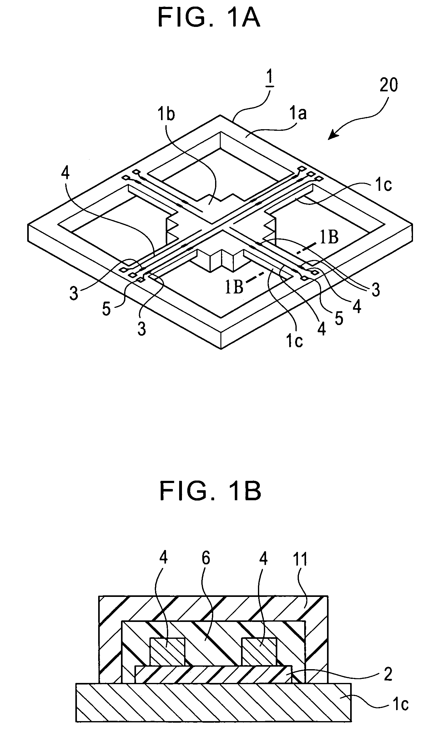
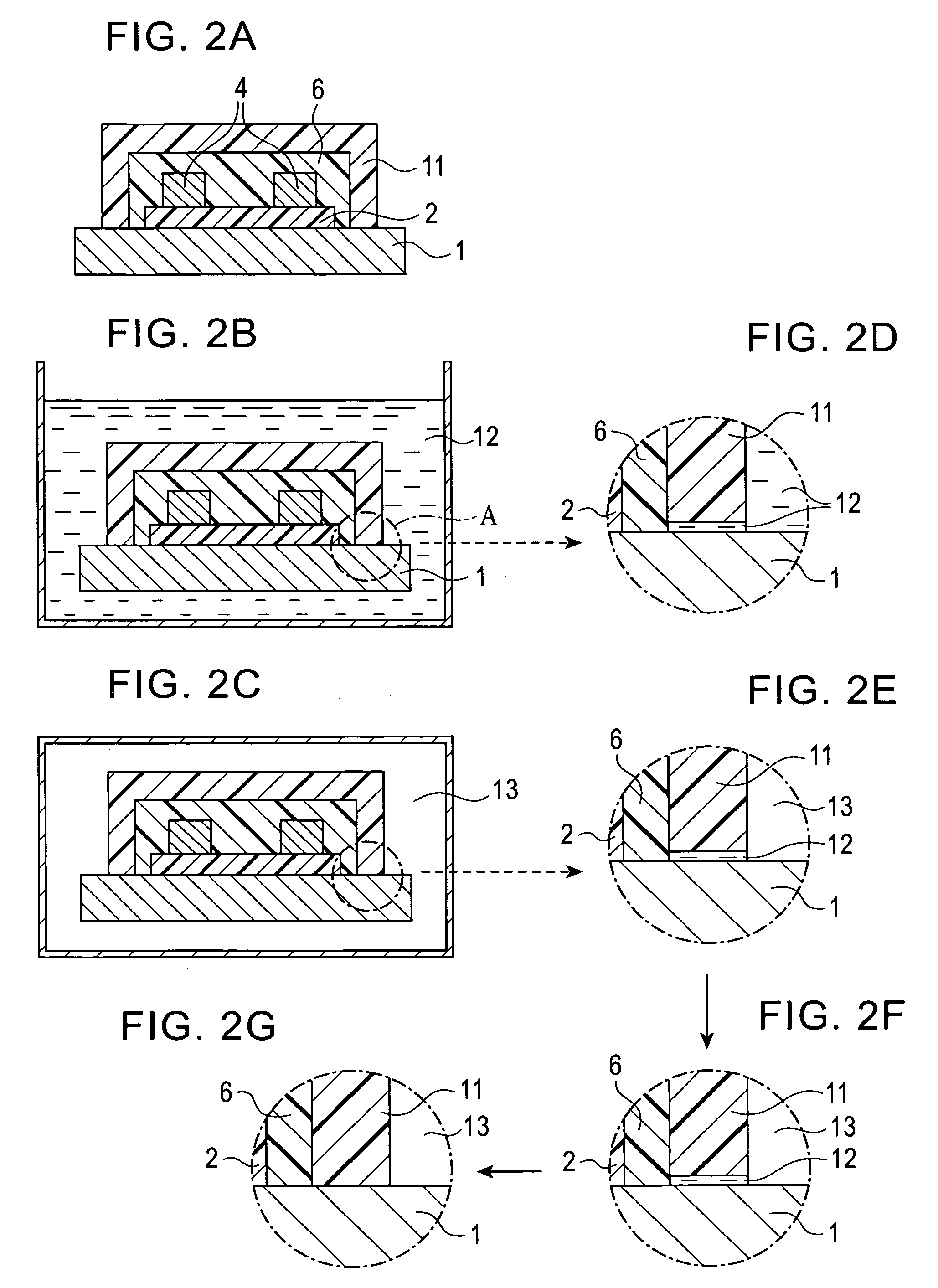
[0023]Referring to FIG. 2A to FIG. 2G, a semiconductor device fabrication method according to Embodiment 1 of the present invention will be described. In this embodiment, the semiconductor device is the acceleration sensor, and the semiconductor device fabrication method will be described using the acceleration sensor shown in FIG. 1A and FIG. 1B.

(1) Step 1 (Resist Forming Processing)

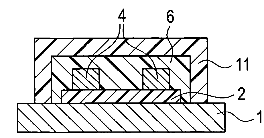
[0024]As FIG. 2A and FIG. 1A show, the piezo resistors 3 and aluminum interconnects 4 are formed on the insulation film 2 made of SiO2. The insulation film 2 is formed on the surface of the silicon substrate (beam sections) 1. The insulation film 2 and aluminum interconnects 4 are covered by protective film 6 for protecting them from corrosion. Then the silicon between the outer frame section 1a and weight section 1b is removed by etching leaving the beam sections 1c, so as to create a space where the weight section 1b can displace according to acceleration. In order to perform cleaning to remove foreig...

embodiment 2

[0031]FIG. 3A to FIG. 3F are diagrams of the semiconductor device fabrication method according to Embodiment 2 of the present invention. The second embodiment has Steps 2a and 2b. Step 2a and Step 2b are additional steps executed between Step 2 and Step 3 of Embodiment 1. Alternatively, it can be said that Step 2 of Embodiment 1 is performed by three steps: the first pure water dipping processing (Step 2), surface active agent dipping processing (Step 2a) and the second pure water dipping processing (Step 2b).

[0032]The following description deals with only the differences between the first embodiment and second embodiment to avoid redundant explanation.

[0033]When Step 2 (pure water dipping process) of Embodiment 1 is performed, that is, when the semiconductor device of which circuit area (e.g., protective film 6) on the substrate 1 is covered with the resist 11 is dipped into the pure water 12 as shown in FIG. 3A, the pure water 12 may not filter into the gap between the silicon sub...

embodiment 3

[0038]FIG. 4A to FIG. 4F are diagrams of the semiconductor device fabrication method according to Embodiment 3 of the present invention. The third embodiment has an etchant dipping processing Step 2ax. Step 2ax is a step performed between step 2a and step 2b of Embodiment 2. It can be said that step 2 of Embodiment 1 is performed by four steps: the first pure water dipping processing (Step 2), surface active agent dipping processing (Step 2a), etchant dipping processing (Step 2ax), and second pure water dipping processing (Step 2b). The following description deals with only the difference between the foregoing embodiments and third embodiment.

Step 2ax (Etchant Dipping Processing)

[0039]After Step 2a of Embodiment 2, i.e., after the surface active agent 14 is filtered into the gap between the semiconductor substrate 1 and the resist 11, the semiconductor device is dipped in an HF aqueous solution 15, of which concentration is about 5%, for a short time (e.g., 120 seconds or about 2 mi...


PUM


Abstract

Circuit elements, such as aluminum interconnects, and a protective film for protecting these circuit elements are formed on a surface of a semiconductor substrate. Resist is formed covering the protective film. The semiconductor substrate on which the resist covering the protective film is formed is dipped into pure water so as to allow the water to filter into a gap between the resist and semiconductor substrate. Then the semiconductor substrate having the resist thereon is dried in high temperature air, and the resist is adhered to the semiconductor substrate by a sticking function due to the surface tension generated when the water is decreasing. The semiconductor substrate to which the resist is adhered is cleaned by a hydrogen fluoride aqueous solution.

Description

BACKGROUND OF THE INVENTION[0001]1. Field of the Invention[0002]The present invention relates to a semiconductor device fabrication method, and more particularly to an HF (hydrogen fluoride) cleaning technology used in the fabrication method.[0003]2. Description of the Related Art[0004]FIG. 1A and FIG. 1B of the accompanying drawings depict an acceleration sensor 20 which is formed by processing a silicon substrate. FIG. 1A is a perspective view and FIG. 1B is a partial cross-sectional view taken along the 1B-1B line in FIG. 1A.[0005]This acceleration sensor 20 has an outer frame section 1a, a weight section 1b and beam sections 1c. These sections are integrated by processing a silicon substrate 1. The outer frame section 1a supports the weight section 1b formed at the center via the flexible four beams 1c. [0006]On the surface of each beam section 1c, an insulation film 2 made of SiO2 is formed, and piezo resistors3 are provided on the insulation film 2. The resistance values of th...

Claims


Application Information

Patent Timeline
Patent Type & Authority Patents(United States)
IPC IPC(8): H01L21/00
CPCG03F7/168H01L21/304
Inventor YOSHIDA, MASASHI
Owner LAPIS SEMICON CO LTD
Learn More